


论文分享
【会员论文】重庆师范大学叶利娟/余鹏/李万俊Optics Letters: 热氧化制备β-Ga₂O₃/GaN异质结用于宽光谱自供电紫外探测
日期:2025-10-21阅读:635
重庆师范大学李万俊教授团队(宽带隙半导体材料与器件团队)在热氧化制备β-Ga2O3/GaN异质结及其宽光谱自供电紫外探测研究中取得进展。相关成果以“Thermal Oxidation–Enabled β-Ga2O3/GaN Heterojunction for Broadband Self-Powered UV Detection”为题发表在《Optics Letters》杂志上。团队研究生蒋佶利为第一作者,叶利娟副教授、余鹏教授和李万俊教授为共同通讯作者。
研发高性能、自供能的宽光谱紫外(UV)光电探测器(PD),对于光谱分析、多光谱成像等应用至关重要。结合多种宽禁带材料的异质结光电探测器,能够拓展紫外探测波长范围,因此在宽光谱紫外探测领域应用广泛。β-Ga2O3与GaN因具备优异的紫外响应特性、热稳定性及化学稳定性,成为紫外探测的理想候选材料。前期,团队已研发出垂直层状结构的 β-Ga2O3/GaN MSM型紫外光电探测器,该器件在施加偏压后展现出均匀宽光谱紫外探测能力。然而,β-Ga2O3/GaN基宽光谱紫外光电探测器的研究仍面临以下挑战:1)GaN外延薄膜热氧化制备β-Ga2O3的质量有待提升;2)自供电宽光谱紫外光电探测器的实现难度较大。为解决上述挑战,本文提出通过热氧化法制备β-Ga2O3/GaN异质结自供能宽光谱紫外光电探测器,主要结论包括:
1. 高性能自供电宽光谱紫外响应:通过热氧化法制备的高结晶度β-Ga2O3,结合湿法刻蚀工艺,使所制备的光电探测器实现了从UV-A到UV-C波段的自供电宽光谱紫外探测。在254 nm光照下,该器件表现出优异性能:响应度达153.9 mA/W,比探测率达1.25×10¹² Jones,外量子效率(EQE)高达75.1%;在365 nm光照下,器件性能同样出色,响应度、比探测率及外量子效率分别达到52.3 mA/W、4.25×10¹¹ Jones和25.6%。该器件的性能具有竞争力,可与通过金属有机化学气相沉积等方法制备的器件相媲美。
2. 单像素扫描成像应用潜力:将β-Ga2O3/GaN自供电宽光谱紫外光电探测器成功应用于单像素紫外成像,获得了高分辨率、高对比度且轮廓清晰的图像。
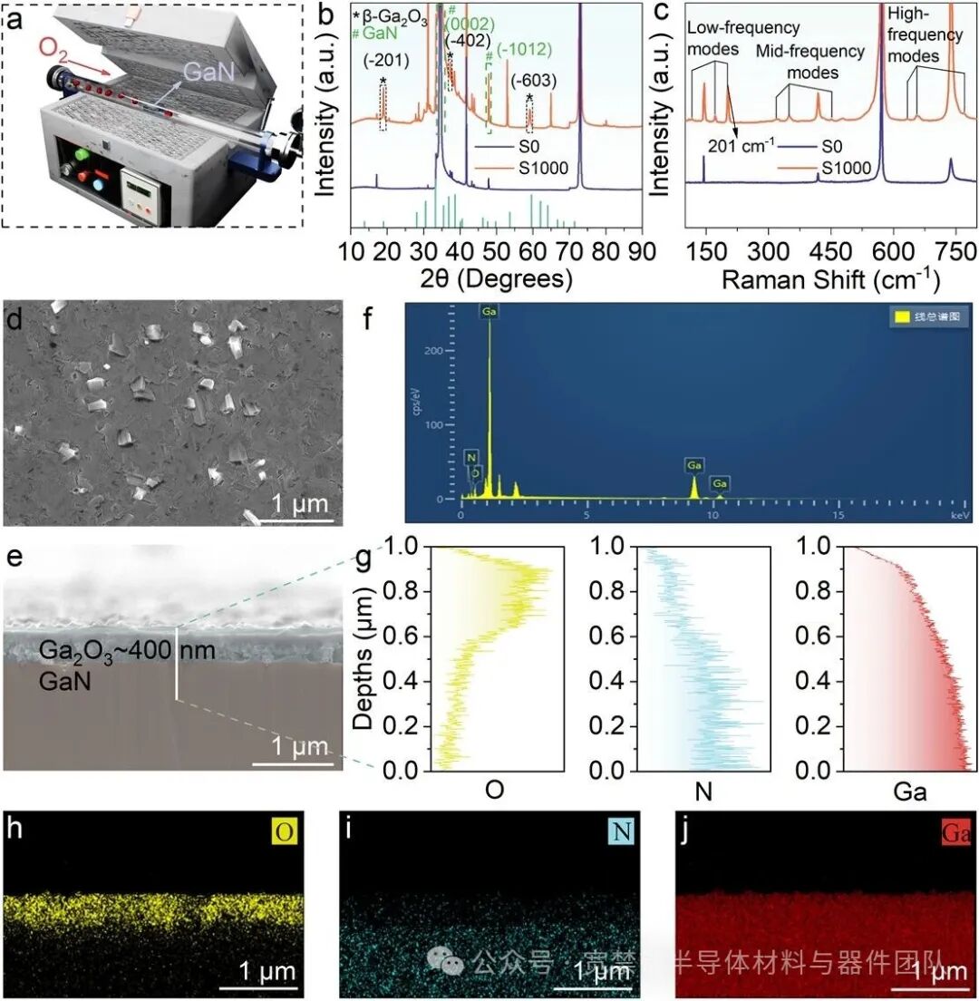
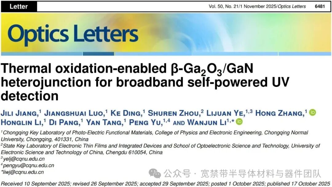
Fig. 1. (a) Thermal oxidation of a GaN thin film in a tube furnace. (b) XRD of S0 (pre-oxidation) and S1000 (oxidized at 1000 °C). (c) Raman spectra of S0 and S1000. (d, e) Surface and cross-sectional SEM of S1000. (f) EDS spectra of S1000. (g–j) Line-scan profiles and elemental maps of O, N, and Ga in the cross-section of S1000.
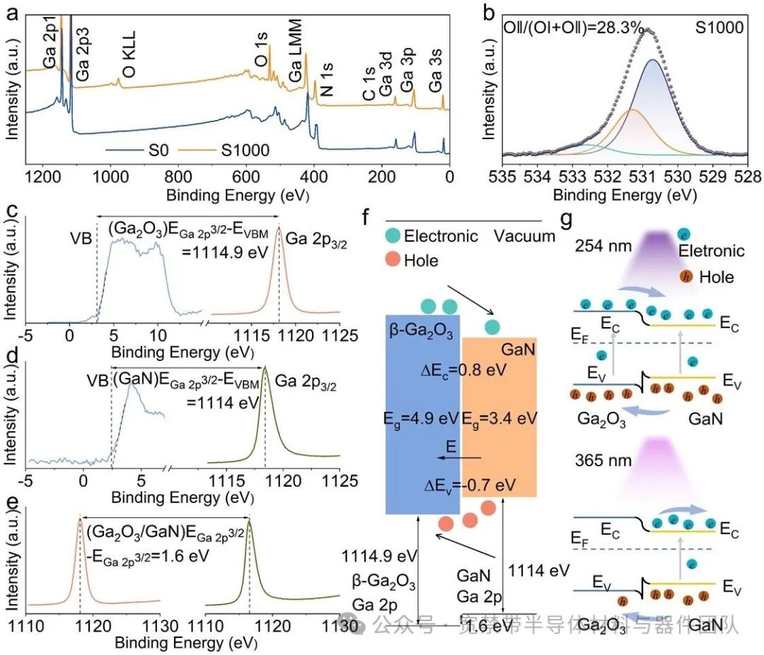
Fig. 2. (a) XPS survey of S0 and S1000. (b) O 1s spectrum of S1000 with peak fitting. (c) Ga 2p3/2 and valence band spectra of S1000. (d) Ga 2p3/2 and valence band spectra of S0. (e) Ga 2p3/2 spectra of S0 and S1000. (f) Band alignment diagram of the β-Ga2O3/GaN heterojunction. (g) Carrier transport mechanisms under 254 and 365 nm UV illumination.
Fig. 3. (a) Schematic of the self-powered Ga2O3/GaN heterojunction photodetector. (b) Spectral responsivity at 0 V. (c) I–V curves under 254 nm illumination with varying power densities. (d) I–V curves under 365 nm illumination with varying power densities. (e) Power-law fitting of photocurrent versus power density at 254 and 365 nm (0 V). (f) I–T curve under 254 nm at 0 V. (g) I–T curve under 365 nm at 0 V.
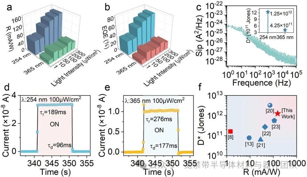
Fig. 4. (a)-(b) R and EQE under 254 nm and 365 nm illumination. (c) Noise power spectral density; the inset (top right) shows the calculated D* derived from the noise spectrum. (d)-(e) Temporal response (rise/fall time) under 254 nm and 365 nm illumination, respectively. (f) Comparison of R and D* for comparable photodetectors.
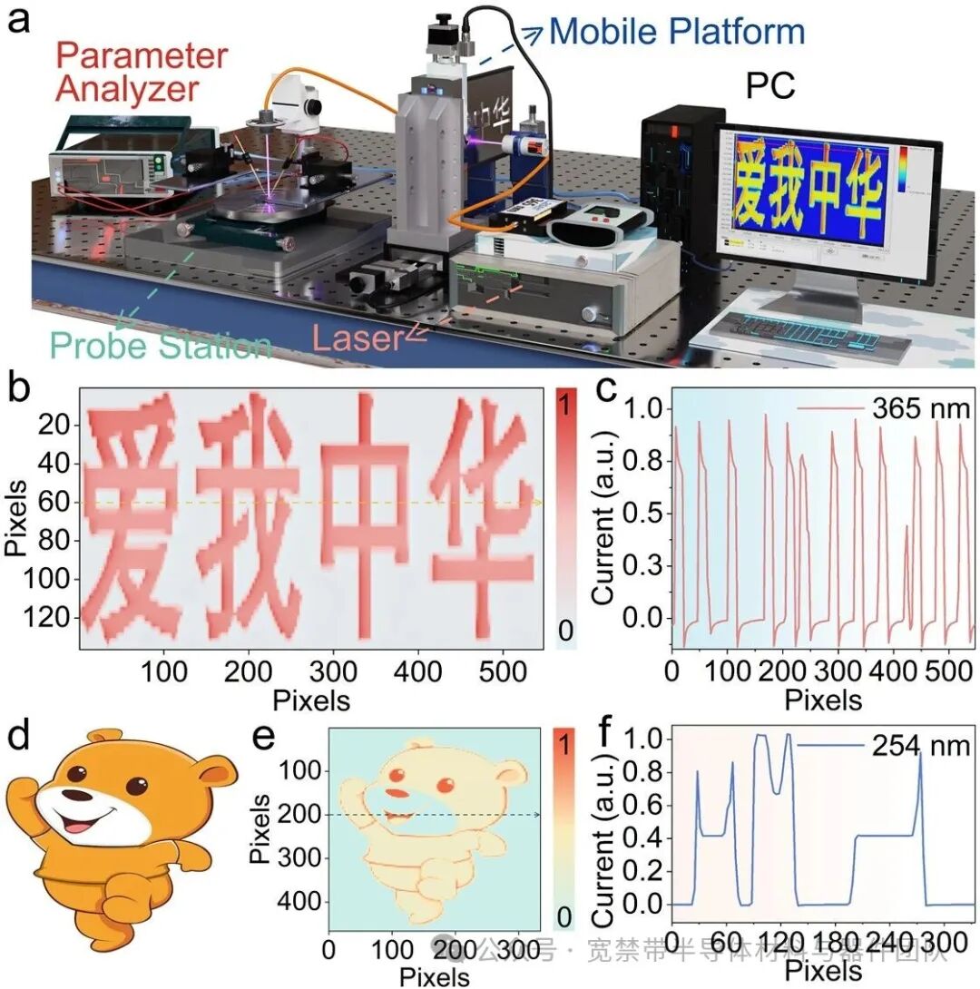
Fig. 5. (a) Schematic of the device integrated into a single-pixel imaging system. (b) Imaging of the Chinese characters “爱我中华” under 365 nm UV. (c) Photocurrent profile during horizontal scanning at the 60th vertical pixel under 365 nm UV illumination. (d) Imaging of a bear-shaped pattern under 254 nm UV. (e) Photocurrent profile during horizontal scanning at the 200th vertical pixel under 254 nm UV illumination.
论文链接:
https://doi.org/10.1364/OL.578462
