


论文分享
【会员论文】西安电子科技大学陆小力&何云龙等:MOCVD外延的(010) β-Ga₂O₃中原位寄生微结构界面与缺陷形成机制研究
日期:2025-01-22阅读:1055
近日,西安电子科技大学陆小力教授、何云龙副教授和西安邮电大学王湛副教授等人在 Science China Materials 发表研究论文,对 MOCVD 外延生长的 (010) β-Ga2O3 薄膜中的界面缺陷形貌结构及形成机理进行了系统分析。
本文要点
1) 通过观测发现了一种丘状表面缺陷,该缺陷呈多边形,并沿 [001] 方向呈现出脊状凸起。透射电子显微(TEM)微观分析表明,多边形丘状缺陷由孪晶组成,呈倒金字塔形嵌入外延层中,并沿 [100] 晶向具有二重旋转对称性。缺陷晶格与完美晶格之间的边界呈带状,伴随复杂的位错结构,其孪晶区与基体的结构关系被确定为 [001]Matrix || [010]Defect 和 {−310}Matrix || {−201}Defect。
2) (010) β-Ga2O3 同质外延层中的表面缺陷成因不仅与衬底缺陷有关,还受到外延工艺条件的影响。
3) 最后,通过 EDX 分析和实验证实,缺陷的形成可能主要归因于生长过程中镓原子和/或氧空位的局部聚集。
该研究为 β-Ga2O3 外延薄膜中的缺陷机制提供了全新的视角,并为 Ga2O3 材料外延技术改进以及功率器件性能提升奠定了重要基础。
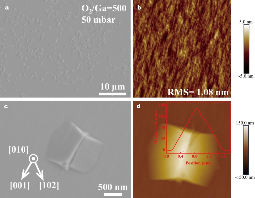
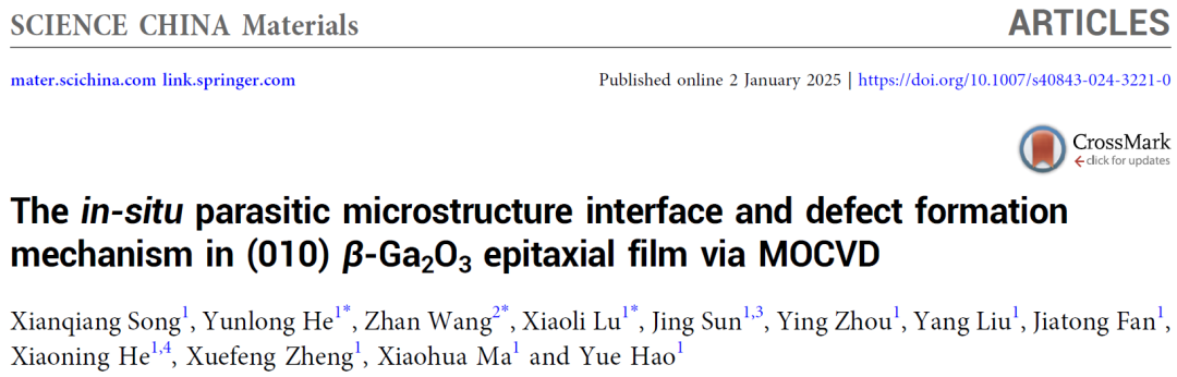
Figure 1. (a) SEM image of the surface of (010) β-Ga2O3 homoepitaxial film with dense polygonal hillock defects. (b) AFM image of an area (5 μm × 5 μm) without defects. (c) High-magnification SEM image of a polygonal hillock defect. (d) AFM image and the height profile of a polygonal hillock defect.
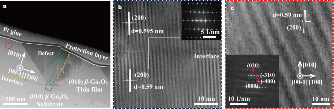
Figure 2. (a) Cross-sectional TEM image of a polygonal hillock defect. (b) HRTEM image of the film-substrate interface, highlighted by the dark blue dashed box in (a). (c) HRTEM image of β-Ga2O3 homoepitaxial layer indicated by the red dashed box in (a), and the inset shows the selected electron diffraction pattern.
Figure 3. (a) HRTEM image at the boundary of the twin inside the polygonal hillock defect marked by the green dashed line box in Fig. 2a. (b) Diffraction pattern showing [010] orientation circled in blue and [0−10] orientation circled in red, with hklL and hklR exhibiting mirror symmetry. (c) A stick and ball model of the observed twin boundary. Bright green and red balls correspond to Ga and O atoms, respectively.
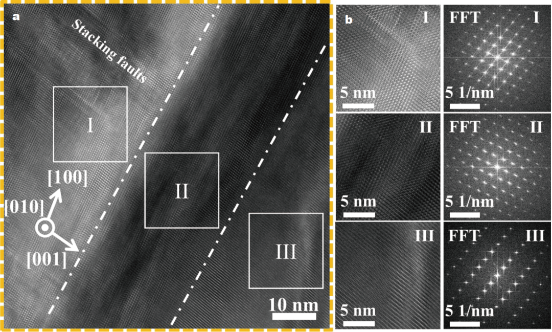
Figure 4. (a) HRTEM image of the yellow boxed area in Fig. 2a, in which there exists a boundary that divides the right twin region into two parts. (b) Enlarged image and FFT pattern of regions I, II and III.
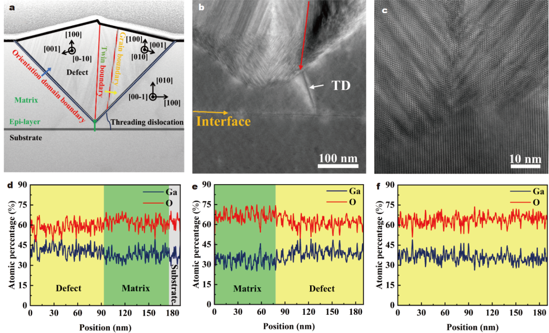
Figure 5. (a) Schematic cross section of the polygonal hillock defect. (b) Magnified TEM image and (c) HRTEM image of the bottom area of the polygonal hillock defect. The STEM-EDX quantification line profiles (d) at the interface between the matrix and the defect, (e) at the boundary studied in Fig. 4, and (f) at the bottom of the defect show the atomic percentages of Ga (blue) and O (red), and the specific scanning positions are indicated by green, blue, and yellow arrows in (a).
文章信息
Xianqiang Song, Yunlong He, Zhan Wang, Xiaoli Lu, Jing Sun, Ying Zhou, Yang Liu, Jiatong Fan, Xiaoning He, Xuefeng Zheng, Xiaohua Ma, Yue Hao. The in-situ parasitic microstructure interface and defect formation mechanism in (010) β-Ga2O3 epitaxial film via MOCVD. Sci. China Mater. (2024).
https://doi.org/10.1007/s40843-024-3221-0
