


论文分享
【会员论文】重庆师范大学张红/李泓霖/李万俊Sci China Mater: 梯度Sn掺杂β-Ga₂O₃构建全空间内建电场助力高性能紫外探测
日期:2025-10-17阅读:622
重庆师范大学李万俊教授团队(宽带隙半导体材料与器件团队)在梯度掺杂调控β-Ga₂O₃光阳极用于自供能日盲紫外光电探测研究中取得进展。相关成果以“Full-space built-in electric field inside gradient Sn-doped β-Ga2O3 photoanodes for enhanced photoelectrochemical solar-blind UV photodetection”为题发表在《Science China Materials》杂志上。团队研究生翟柯为第一作者,张红副教授、李泓霖教授和李万俊教授为共同通讯作者。
自供电光探测器在构建未来光电子系统中具有关键作用,尤其适用于环境监测、安全通信和水下成像等应用领域。其中,光电化学(PEC)型日盲紫外探测器(200-280 nm),因其巧妙融合了半导体物理特性与化学反应过程,展现出卓越的的自供电能力、简易制备、低成本及环境友好等优势。在金属氧化物半导体中,β-Ga2O3凭借4.9 eV的合适带隙、优异的光响应特性及高稳定性,成为日盲紫外检测的理想候选材料。然而,基于β-Ga2O3的光电化学探测器研究仍面临以下挑战:1)由于缺乏足够驱动力,导致光生载流子分离和转移效率低下。2)传统均匀掺杂策略形成的内建电场作用范围有限,无法有效抑制体相复合。
为突破这些限制,团队提出梯度掺杂策略,通过构建空间梯度能带结构,形成全空间内建电场,显著增强了电荷分离与传输。本方案结合溶胶-凝胶法与快速热退火技术,实现锡元素的可控梯度掺杂,有效解决了体相掺杂的系列缺陷。主要成果如下:1)梯度锡掺杂在β-Ga2O3光阳极中成功诱导出贯穿全空间的内建电场,在抑制体相复合的同时为电荷分离提供了额外驱动力。2)梯度诱导的内建电场与半导体/电解质界面处的内建电场方向一致,形成连续的电荷传输通道,进而实现卓越的光探测性能。3)梯度掺杂光阳极展现出66.88 mA/W的优异响应度与79/65 ms的快速上升/下降时间,并成功实现水下紫外成像。
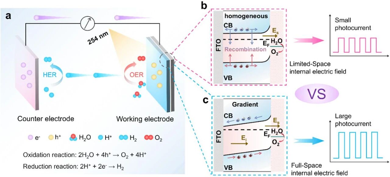
Figure 1. Energy band diagrams. (a) Schematic illustration of the PEC-type photodetector. Band bending schematics and the resulting photocurrents of (b) homogeneous doped photoanode and (c) gradient-doped photoanode. CB, conduction band; VB, valence band; EF, Fermi level; Ei, electric field arising from the gradient doping; Es, electric field arising from the β-Ga2O3/electrolyte junction.
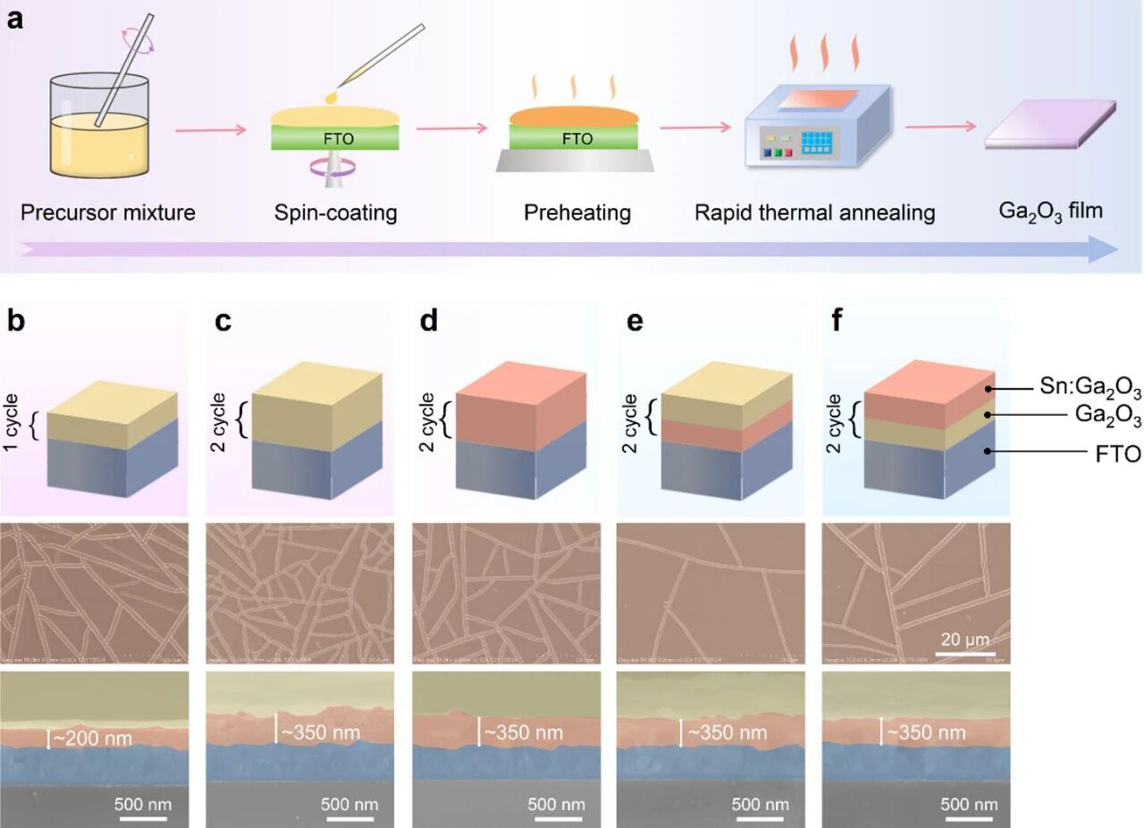
Figure 2. Schematic diagrams of Sn-doped Ga2O3 films. (a) Fabrication process of β-Ga2O3 films via sol-gel method. Schematic of the β-Ga2O3 films prepared with (b) one cycle, (c) two cycles, (d) homogeneous, (e) gradient, and (f) reverse gradient Sn doping; the corresponding SEM images are also included.
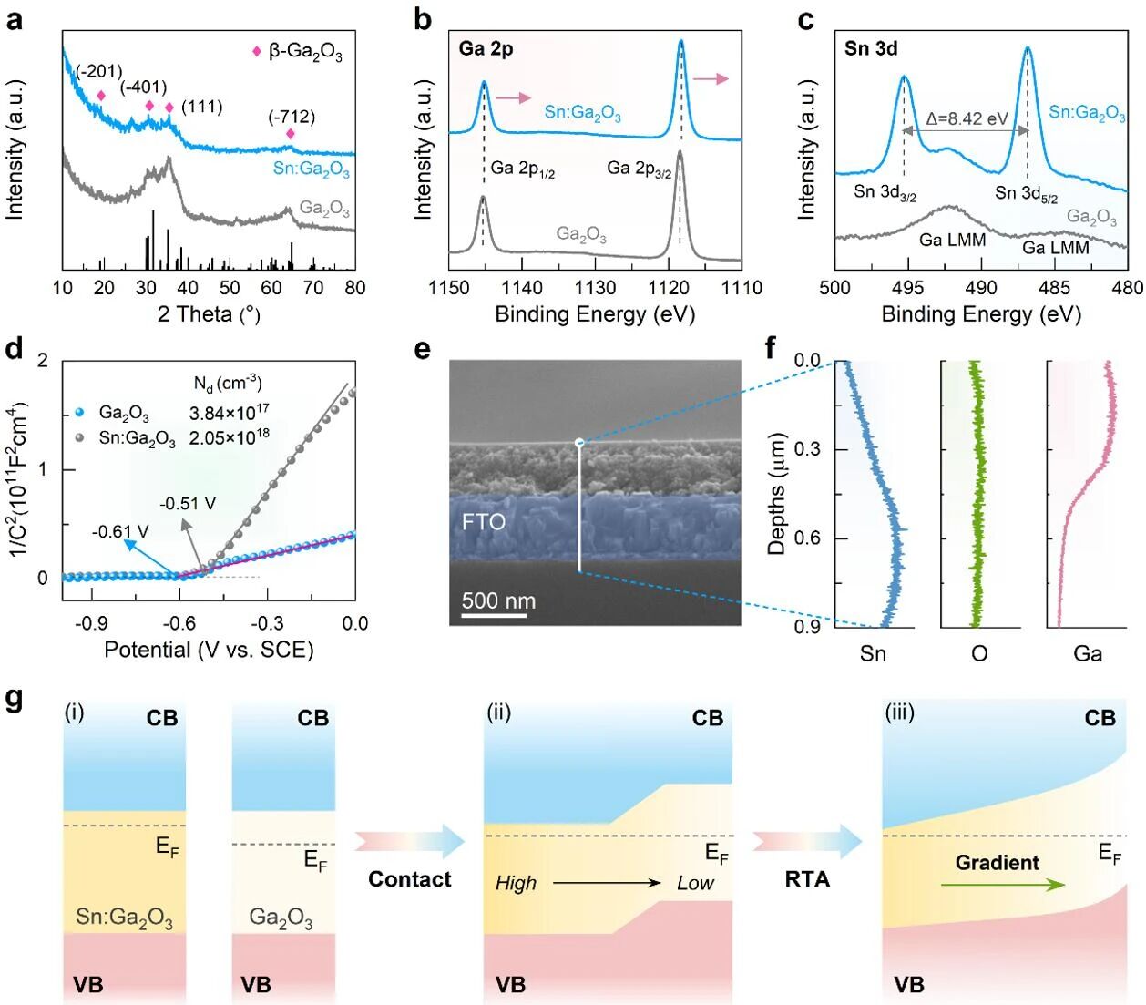
Figure 3. Material characterizations. (a) GIXRD patterns, (b) Ga 2p core-level XPS spectra, (c) Sn 3d core-level XPS spectra, and (d) Mott-Schottky curves of the Ga2O3 film and the Sn:Ga2O3 film with a Sn content of 6%. (e) Cross-sectional SEM image and (f) EDS linear scan profile of the gradient Sn:Ga2O3 film. (g) Schematic band alignments of gradient Sn:Ga2O3 film before contact (i), after contact (ii), and the formed full-space electric field after rapid thermal annealing (iii).
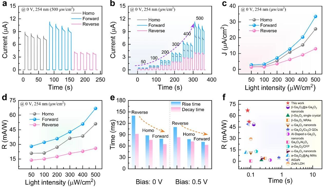
Figure 4. Evaluation of self-powered PEC performance. (a) I-t curves of homogeneous, gradient, and reverse gradient Sn:Ga2O3 films under 254 nm (500 μW/cm2) illumination and 0 V bias in 0.5 M Na2SO4. (b) I-t curves and (c) corresponding photocurrent density under various light intensities. (d) Calculated responsivity values as a function of incident light intensities. (e) Response time under 0 V and 0.5 V. (f) Performance comparisons of PEC-type UV photodetectors in this work and other reported device.
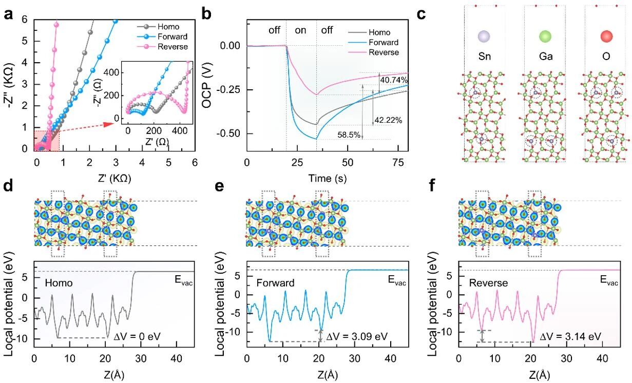
Figure 5. Characterization of charge carrier dynamic and electronic structure properties. (a) EIS profiles of homogeneous, gradient, and reverse gradient Sn:Ga2O3 photoanodes; the inset shows the enlarged view of the high-frequency region in EIS profiles. (b) Open circuit potential (OCP) plots. (c) Optimized structure of β-Ga2O3 photoanode with (left) homogeneous, (middle) gradient, and (right) reverse gradient Sn doping. (d–f) 3D charge density difference and plane-averaged electrostatic potential drop across the interface for (d) homogeneous, (e) gradient, and (f) reverse gradient Sn:Ga2O3 photoanodes. Evac represent the vacuum level.
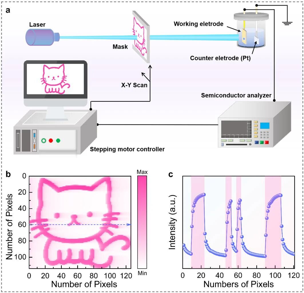
Figure 6. Schematic representation of the device application. (a) Schematic diagram of the underwater optical imaging system. (b) Image obtained from the image scanning system. (c) Cross section of continuous current value at straight line position in (b).
论文信息:
Ke Zhai, Hong Zhang*, Shiyi Li, Jieneng Chen, Pukai Zhou, Hang Cui, Di Pang, Yan Tang, Lijuan Ye, Honglin Li* and Wanjun Li*. Full-space built-in electric field inside gradient Sn-doped β-Ga2O3 photoanodes for enhanced photoelectrochemical solar-blind UV photodetection. Science China Materials, 2025, DOI: 10.1007/s40843-025-3757-2.
论文链接:
https://doi.org/10.1007/s40843-025-3757-2
