


论文分享
【会员论文】重庆师范大学唐燕/李万俊CEJ:Cu@CuOₓ@a-Ga₂O₃核壳异质纳米线的构筑及其自供电多波段双极性光电探测器
日期:2025-11-13阅读:481
重庆师范大学李万俊教授团队(宽禁带半导体材料与器件团队)在Cu@CuOx@a-Ga2O3核壳异质纳米线的构筑及其自供电多波段双极性光电探测器研究中取得进展。相关成果以“Multiband Bipolar Photoresponse in a Cu@CuOx NWs@a-Ga2O3-Based Self-Powered Photoelectrochemical-type Photodetectors for Secure Underwater Optical Communication”为题发表在《Chemical Engineering Journal》杂志上。团队研究生孙益鑫为第一作者,唐燕博士和李万俊教授为共同通讯作者。
光电化学型双极性光电探测器(PEC-BPDs)凭借对多波段光的极性可调响应特性,为构建安全、多通道且低功耗的水下光通信系统提供了全新路径。本研究设计并构建了一种基于Cu@CuOx@a-Ga2O3核壳异质结构的自供电PEC-BPDs,实现了从深紫外到近红外的宽光谱响应与可逆光电流极性切换。通过调控光生载流子的输运行为,揭示了光波长诱导的光电流反转机制,赋予器件在紫外与紫外、紫外与可见、紫外与近红外等多波段组合下的双极响应能力。在此基础上,不仅在单一器件中实现多种逻辑功能(OR、NOT、XOR、NAND)的切换,还结合交替标记反转(AMI)编码实现了光谱维度的水下加密通信,具备并行信息传输与自主纠错能力。该研究为多功能光电器件设计和智能水下光通信系统的构建提供了新策略,展现了PEC-BPDs在下一代安全水下通信中的应用潜力。
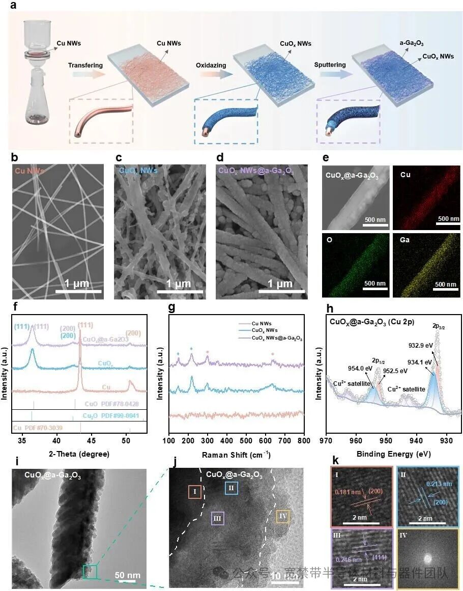
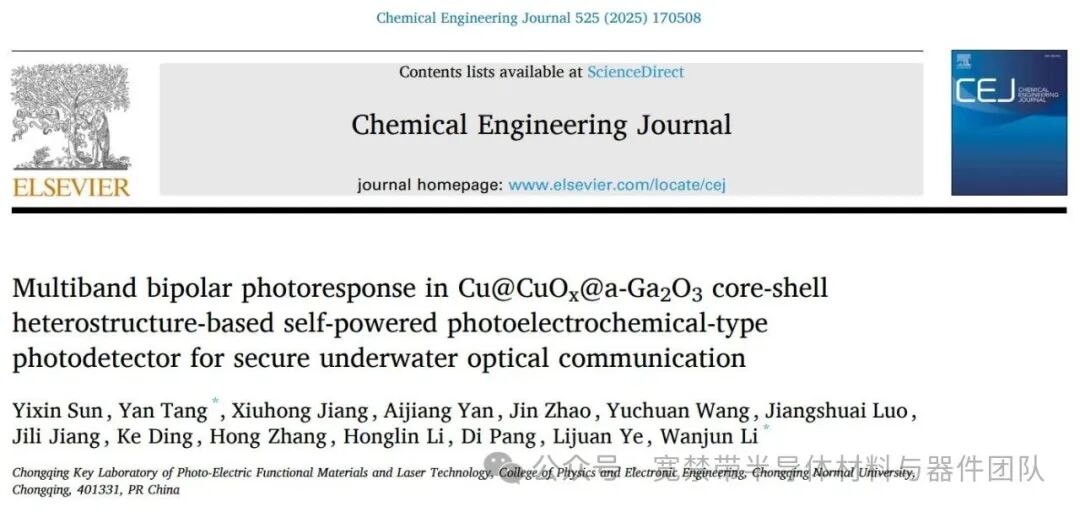
Figure 1. Preparation and characterization of Cu@CuOx@a-Ga2O3 network films. a) Schematic illustration of the preparation process for Cu@CuOx@a-Ga2O3 network films. SEM images of Cu NWs networks b), Cu@CuOx network film c), and Cu@CuOx@a-Ga2O3 network film d). e) SEM image combined EDS elemental mapping of a single Cu@CuOx@a-Ga2O3 nanowire. f) XRD spectrum, g) Raman scattering spectrum of Cu NWs film, Cu@CuOx film and Cu@CuOx@a-Ga2O3 film. h) Cu 2p XPS spectrum of Cu@CuOx@a-Ga2O3. i) TEM image of Cu@CuOx@a-Ga2O3. j) HRTEM image of the green boxed area in (i). k) The magnified regions (I-III) and FFT image (IV) of the corresponding color boxed areas in (i).
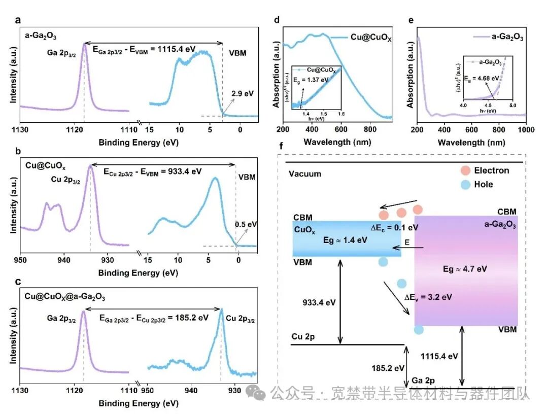
Figure 2. Energy band structure of CuOx@a-Ga2O3. a) Ga 2p3/2 core-level spectrum and valence band spectrum of a-Ga2O3. b) Cu 2p3/2 core-level spectrum and valence band spectrum of Cu@CuOx. c) Ga 2p3/2 and Cu 2p3/2 core-level spectra of Cu@CuOx@a-Ga2O3. d) Absorption spectrum and optical band gap of Cu@CuOx. e) Absorption spectrum and optical band gap of a-Ga2O3. f) Schematic illustration of the energy band alignment of CuOx@a-Ga2O3 in the working electrode.
Figure 3. Investigation on the wavelength-induced bipolar mechanism of Cu@CuOx@a-Ga2O3 PEC-BPDs with varying a-Ga2O3 layer thickness. a) Broad-spectrum photoelectric properties of a-Ga2O3 and Cu@CuOx PEC-PDs (0 V, 0.8 mW/cm2). b) Broad-spectrum photoelectric properties of Cu@CuOx@a-Ga2O3 PEC-BPD (0 V, 0.8 mW/cm2). c) I-t curves under 254 nm light irradiation and d) I-t curves under 365 nm light irradiation of Cu@CuOx@a-Ga2O3 PEC-BPDs with different a-Ga2O3 deposition times (0 V, 0.8 mW/cm2). Band bending and charge transfer under 254 nm light irradiation for Cu@CuOx@a-Ga2O3 films with thin e), medium f), and thick g) a-Ga2O3 layers. Band bending and charge transfer under 365 nm light irradiation for Cu@CuOx@a-Ga2O3 films with thin h), medium i), and thick j) a-Ga2O3 layers.
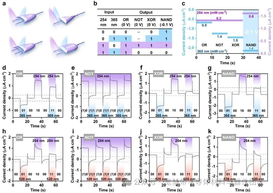
Figure 4. Demonstration of reprogrammable optical switching logic gates based on Cu@CuOx@a-Ga2O3 PEC-BPD with 30 min a-Ga2O3 sputtering time. a) Schematic diagrams of four optical switching logic gates: OR, NOT, XOR, and NAND. b) Truth table of OR, NOT, XOR, and NAND logic gates. c) Photocurrent values of Cu@CuOx@a-Ga2O3 PEC-BPD by single input signals (254 or 365 nm) for different logic gates, with the light intensity and bias voltage of the two signals. I-t curves of OR d), NOT e), XOR f), and NAND g) logic gates with 254 nm and 365 nm illumination. I-t curves of OR h), NOT i), XOR j), and NAND k) logic gates with 254 nm and 520 nm illumination. The on/off states of 254 nm and 365 nm/520 nm LEDs correspond to input logic states of 1/0. For the output photocurrent within the range of -0.25~0.25 μA/cm2, the output state is set as “0”, while the photocurrent outside this range indicates the output state “1”.

Figure 5. Demonstration of the encrypted optical communication system. a) Conceptual diagram of encrypted optical communication system. b) Diagram of AMI code splitting. c) The self-verification mechanism of the system when abnormal signal occurs. The bipolar photocurrent response curves of the Cu@CuOx@a-Ga2O3 PEC-BPD under parallel signal transmission with combined wavelengths of 254 nm and 365 nm d), 254 nm and 520 nm e) to transmitte the information “CQNU”.
DOI:
https://doi.org/10.1016/j.cej.2025.170508
