Paper Sharing
【International Papers】Thin Ga₂O₃ Layers by Thermal Oxidation of van der Waals GaSe Nanostructures for Ultraviolet Photon Sensing
日期:2024-10-31阅读:973
Researchers from the University of Nottingham have published a dissertation titled "Thin Ga2O3 Layers by Thermal Oxidation of van der Waals GaSe Nanostructures for Ultraviolet Photon Sensing" in ACS Applied Nano Materials.
Abstract
Two-dimensional semiconductors (2DSEM) based on van der Waals crystals offer important avenues for nanotechnologies beyond the constraints of Moore’s law and traditional semiconductors, such as silicon (Si). However, their application necessitates precise engineering of material properties and scalable manufacturing processes. The ability to oxidize Si to form silicon dioxide (SiO2) was crucial for the adoption of Si in modern technologies. Here, we report on the thermal oxidation of the 2DSEM gallium selenide (GaSe). The nanometer-thick layers are grown by molecular beam epitaxy on transparent sapphire (Al2O3) and feature a centro-symmetric polymorph of GaSe. Thermal annealing of the layers in an oxygen-rich environment promotes the chemical transformation and full conversion of GaSe into a thin layer of crystalline Ga2O3, paralleled by the formation of coherent Ga2O3/Al2O3 interfaces. Versatile functionalities are demonstrated in photon sensors based on GaSe and Ga2O3, ranging from electrical insulation to unfiltered deep ultraviolet optoelectronics, unlocking the technological potential of GaSe nanostructures and their amorphous and crystalline oxides.
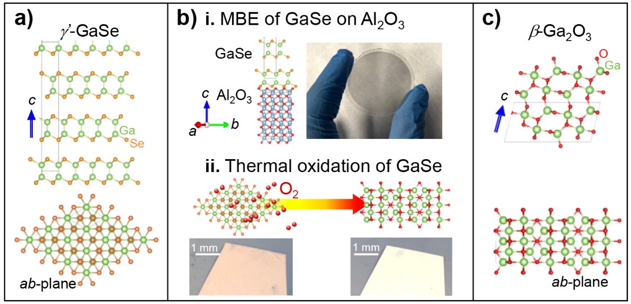
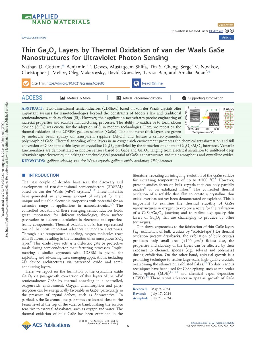
Figure 1. Chemical conversion of MBE-grown GaSe into Ga2O3. (a). Cross-sectional view (top) and planar view (bottom) of the crystal structure of γ′-GaSe. (b) Photograph and schematic of (i) MBE γ′-GaSe on Al2O3 and (ii) optical microscopy images of the surface of γ′-GaSe and β-Ga2O3. The inset in panel (ii) is a schematic of the changes during thermal oxidation of γ′-GaSe and its conversion into β-Ga2O3. (c) Schematic of the cross-sectional view (top) and planar view (bottom) of the crystal structure of β-Ga2O3.
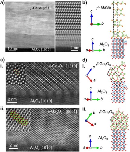
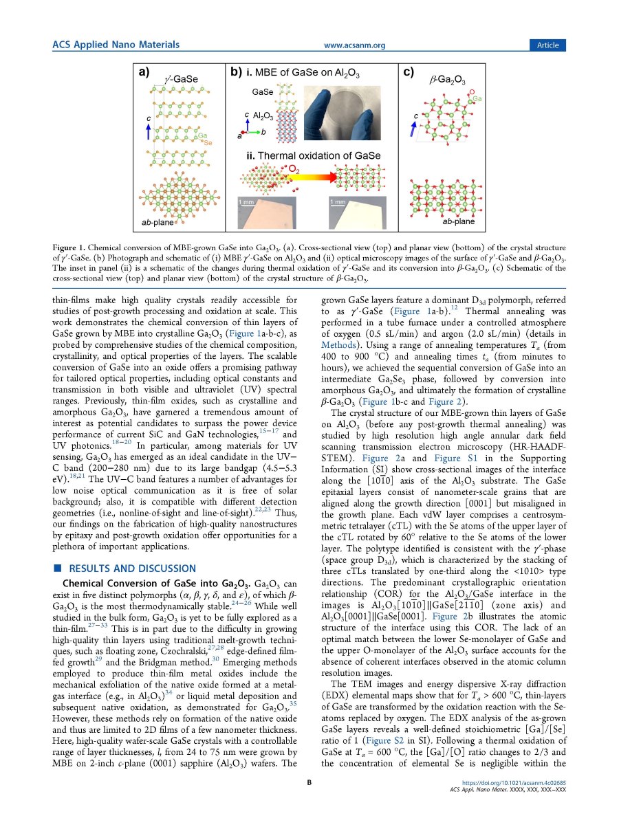
Figure 2. Crystal structures and interfaces of γ′-GaSe and β-Ga2O3 with sapphire. (a) Cross-sectional high resolution (HR) high-angle annular dark-field scanning transmission electron microscopy (HAADF-STEM) images of as-grown γ′-GaSe on sapphire (thickness l = 75 nm). (b) Schematic of the interface of γ′-GaSe on Al2O3. (ci-ii) HR-STEM images showing the formation of coherent interfaces for 2 different crystallographic orientation relationships (COR) of a sample annealed at Ta = 900 °C for ta = 30 min in an Ar/O2 mixture. The superposition of the crystal structures with different orientations of β-Ga2O3 on the enlarged ADF images in the insets show a complete fitting. (di-ii) Schematic of the interface of β-Ga2O3 on Al2O3, as observed in the ADF images for both CORs.
DOI:
https://doi.org/10.1021/acsanm.4c02685