Paper Sharing
【International Papers】Impact of Channel Thickness and Doping Concentration for Normally-Off Operation in Sn-Doped β-Ga₂O₃ Phototransistors
日期:2024-11-21阅读:1170
Researchers from the Korea Aerospace University have published a dissertation titled " Impact of Channel Thickness and Doping Concentration for Normally-Off Operation in Sn-Doped β-Ga2O3 Phototransistors " in Sensors.
Abstract
We demonstrate a Sn-doped monoclinic gallium oxide (β-Ga2O3)-based deep ultraviolet (DUV) phototransistor with high area coverage and manufacturing efficiency. The threshold voltage (VT) switches between negative and positive depending on the β-Ga2O3 channel thickness and doping concentration. Channel depletion and Ga diffusion during manufacturing significantly influence device characteristics, as validated through computer-aided design (TCAD) simulations, which agree with the experimental results. We achieved enhancement-mode (e-mode) operation in <10 nm-thick channels, enabling a zero VG to achieve a low dark current (1.84 pA) in a fully depleted equilibrium. Quantum confinement in thin β-Ga2O3 layers enhances UV detection (down to 210 nm) by widening the band gap. Compared with bulk materials, dimensionally constrained optical absorption reduces electron–phonon interactions and phonon scattering, leading to faster optical responses. Decreasing β-Ga2O3 channel thickness reduces VT and VG, enhancing power efficiency, dark current, and the photo-to-dark current ratio under dark and illuminated conditions. These results can guide the fabrication of tailored Ga2O3-based DUV phototransistors.
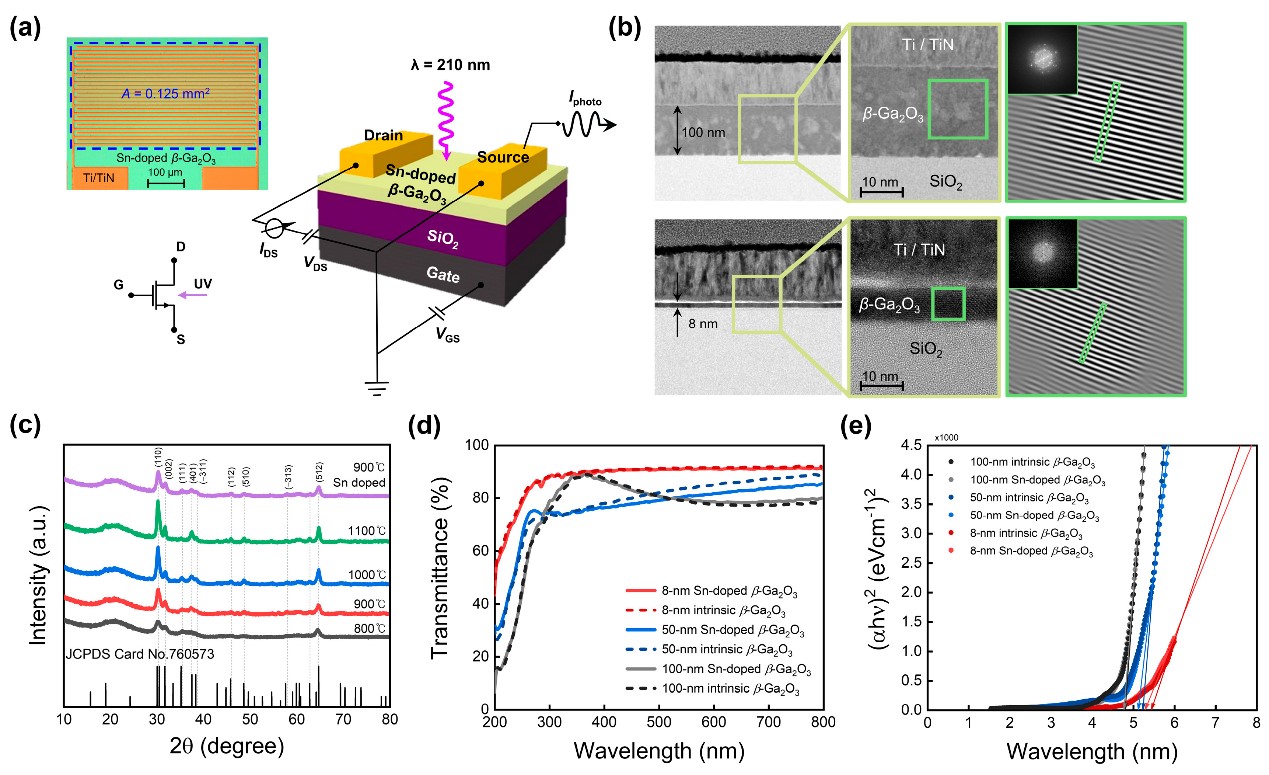
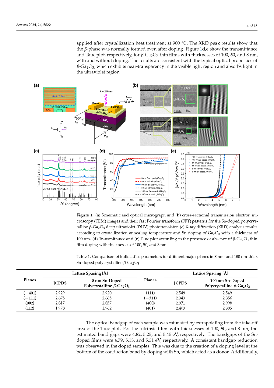
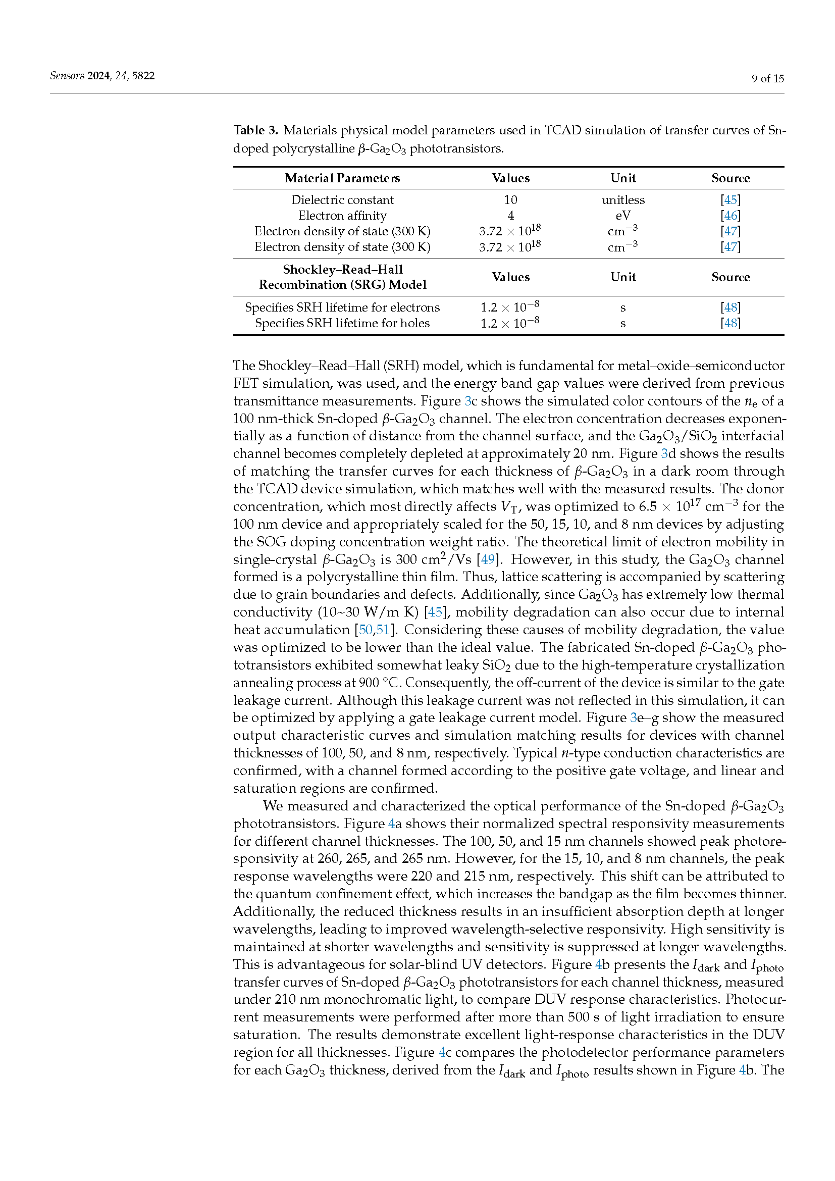
Figure 1. (a) Schematic and optical micrograph and (b) cross-sectional transmission electron microscopy (TEM) images and their fast Fourier transform (FFT) patterns for the Sn-doped polycrystalline β-Ga2O3 deep ultraviolet (DUV) phototransistor. (c) X-ray diffraction (XRD) analysis results according to crystallization annealing temperature and Sn doping of Ga2O3 with a thickness of 100 nm. (d) Transmittance and (e) Tauc plot according to the presence or absence of β-Ga2O3 thin film doping with thicknesses of 100, 50, and 8 nm.
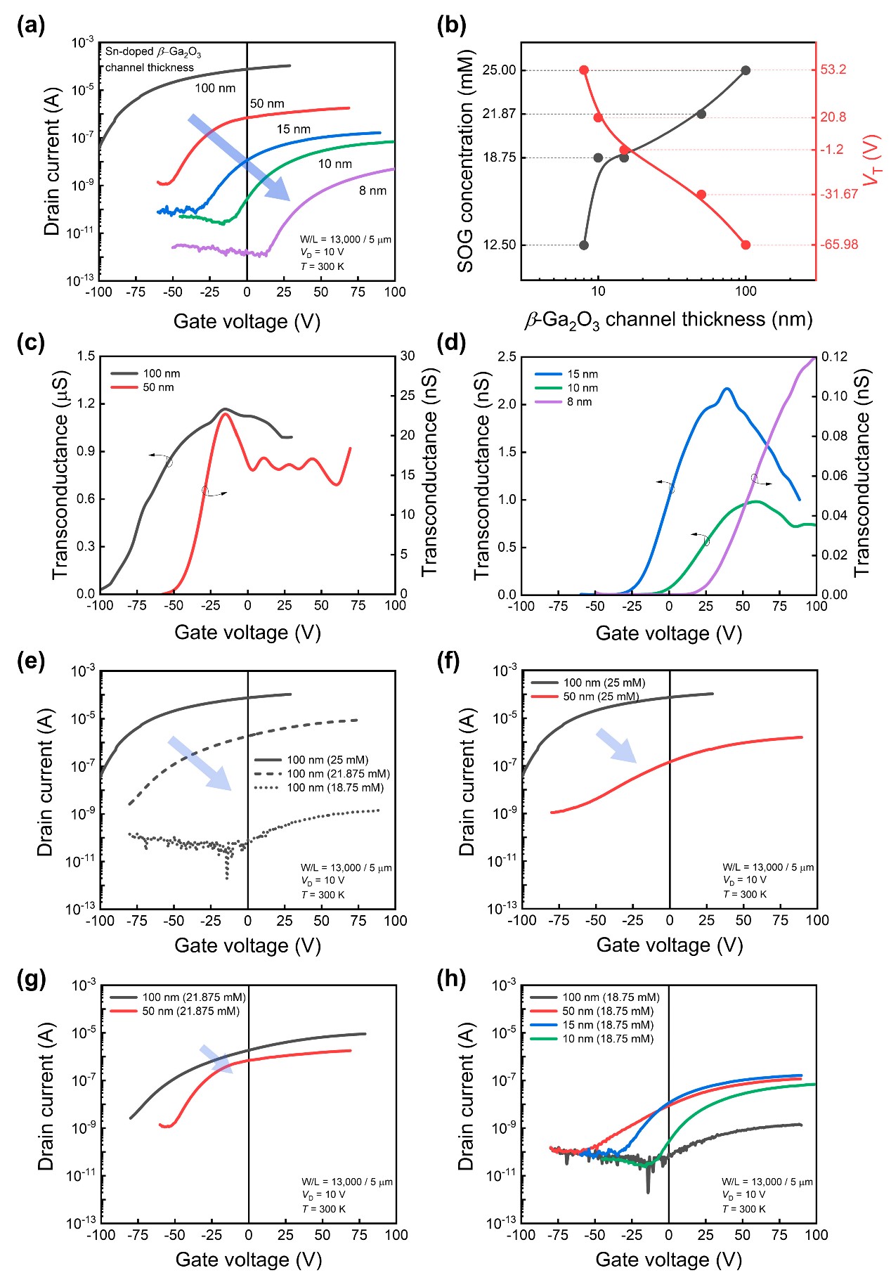
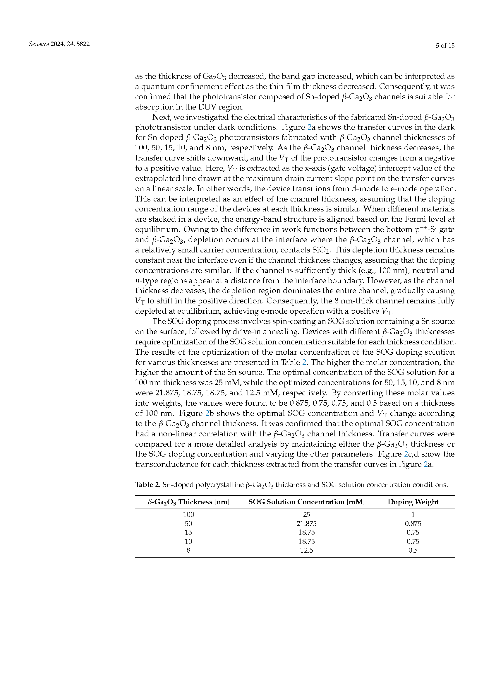
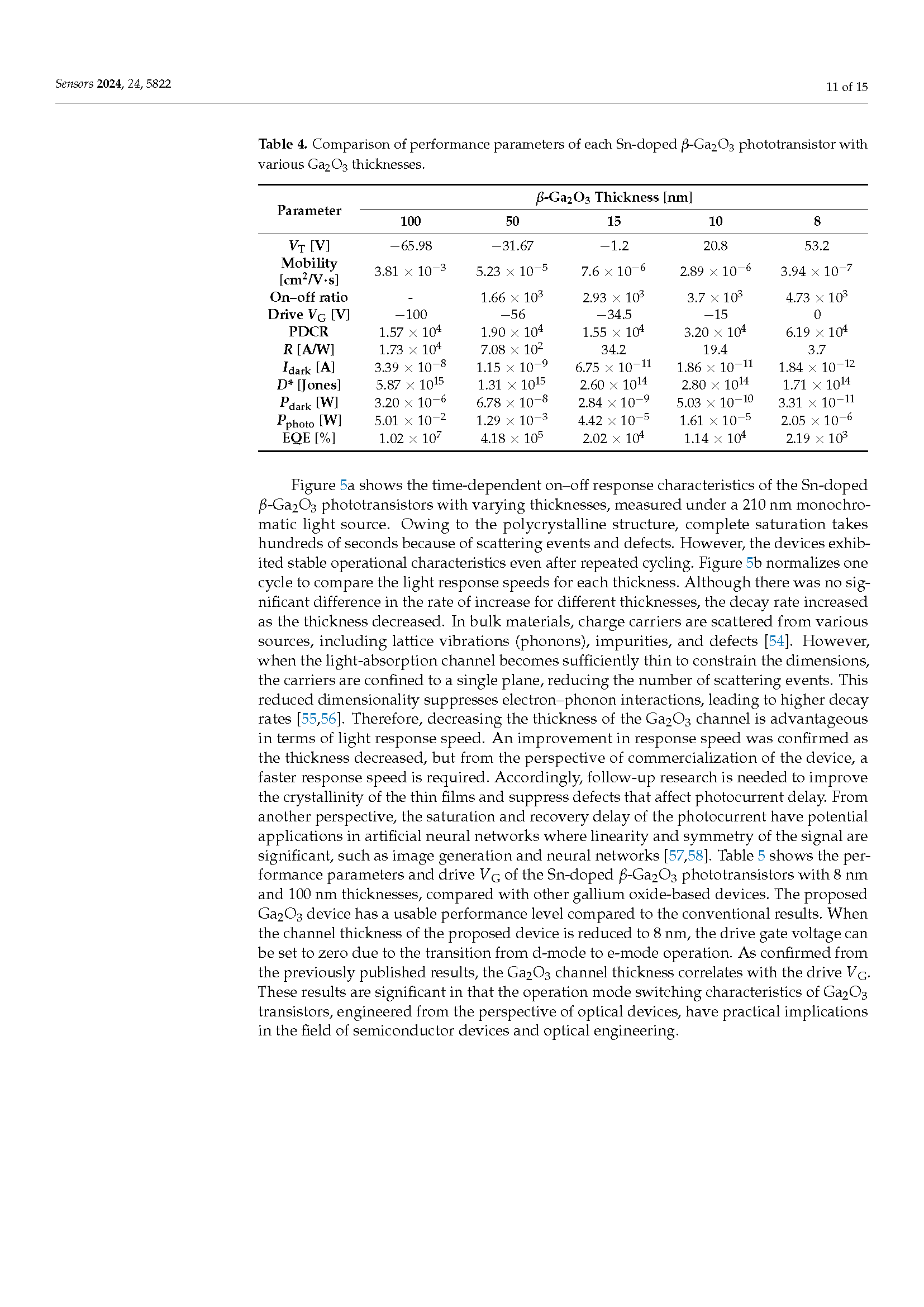
Figure 2. (a) Transfer curves of Sn-doped β-Ga2O3 phototransistors fabricated with β-Ga2O3 channel thicknesses of 100, 50, 15, 10, and 8 nm. (b) Optimal spin-on-glass (SOG) doping concentration and corresponding VT change according to β-Ga2O3 channel thickness. Transconductance for each thickness (c) 100 and 50 nm, (d) 15, 10 and 8 nm. Each data point was calculated from the curves in (a). (e) Changes in transfer curves with a constant thickness of 100 nm and varying SOG doping concentrations. Changes in transfer curves for a constant SOG doping concentration and varying thickness at 100 nm and 50 nm (f) 25 mM, (g) 21.875 mM. (h) Transfer curves for a constant SOG doping concentration at 18.75 mM and varying thickness at 100, 50, 15, and 10 nm.
DOI:
https://doi.org/10.3390/s24175822