Paper Sharing
【Domestic Papers】Research from the South China University of Technology about Ohmic Contact Formation to β-Ga₂O₃ Nanosheet Transistors with Ar-Containing Plasma Treatment
日期:2024-11-21阅读:936
Researchers from the South China University of Technology have published a dissertation titled "Ohmic Contact Formation to β-Ga2O3 Nanosheet Transistors with Ar-Containing Plasma Treatment" in Electronics.
Abstract
Effective Ohmic contact between metals and their conductive channels is a crucial step in developing high-performance Ga2O3-based transistors. Distinct from bulk materials, excess thermal energy of the annealing process can destroy the low-dimensional material itself. Given the thermal budget concern, a feasible and moderate solution (i.e., Ar-containing plasma treatment) is proposed to achieve effective Ohmic junctions with (100) β-Ga2O3 nanosheets. The impact of four kinds of plasma treatments (i.e., gas mixtures SF6/Ar, SF6/O2/Ar, SF6/O2, and Ar) on (100) β-Ga2O3 crystals is comparatively studied by X-ray photoemission spectroscopy for the first time. With the optimal plasma pre-treatment (i.e., Ar plasma, 100 W, 60 s), the resulting β-Ga2O3 nanosheet field-effect transistors (FETs) show effective Ohmic contact (i.e., contact resistance RC of 104 Ω·mm) without any post-annealing, which leads to competitive device performance such as a high current on/off ratio (>107), a low subthreshold swing (SS, 249 mV/dec), and acceptable field-effect mobility (μeff, ~21.73 cm2 V−1 s−1). By using heavily doped β-Ga2O3 crystals (Ne, ~1020 cm−3) for Ar plasma treatments, the contact resistance RC can be further decreased to 5.2 Ω·mm. This work opens up new opportunities to enhance the Ohmic contact performance of low-dimensional Ga2O3-based transistors and can further benefit other oxide-based nanodevices.
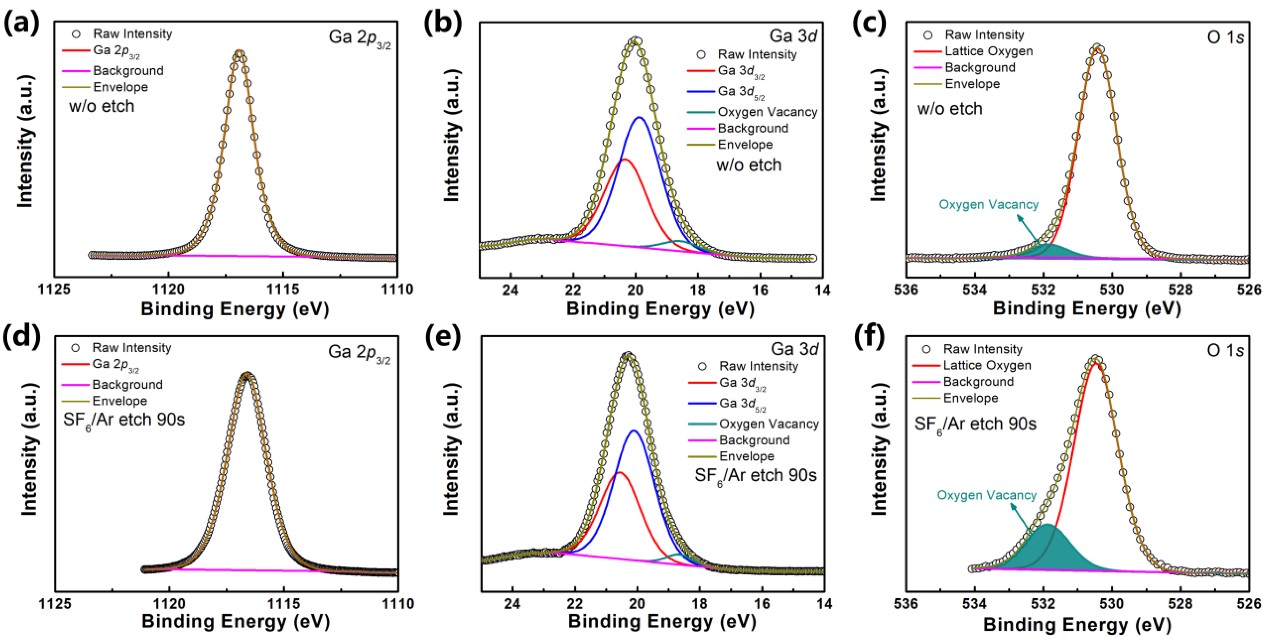
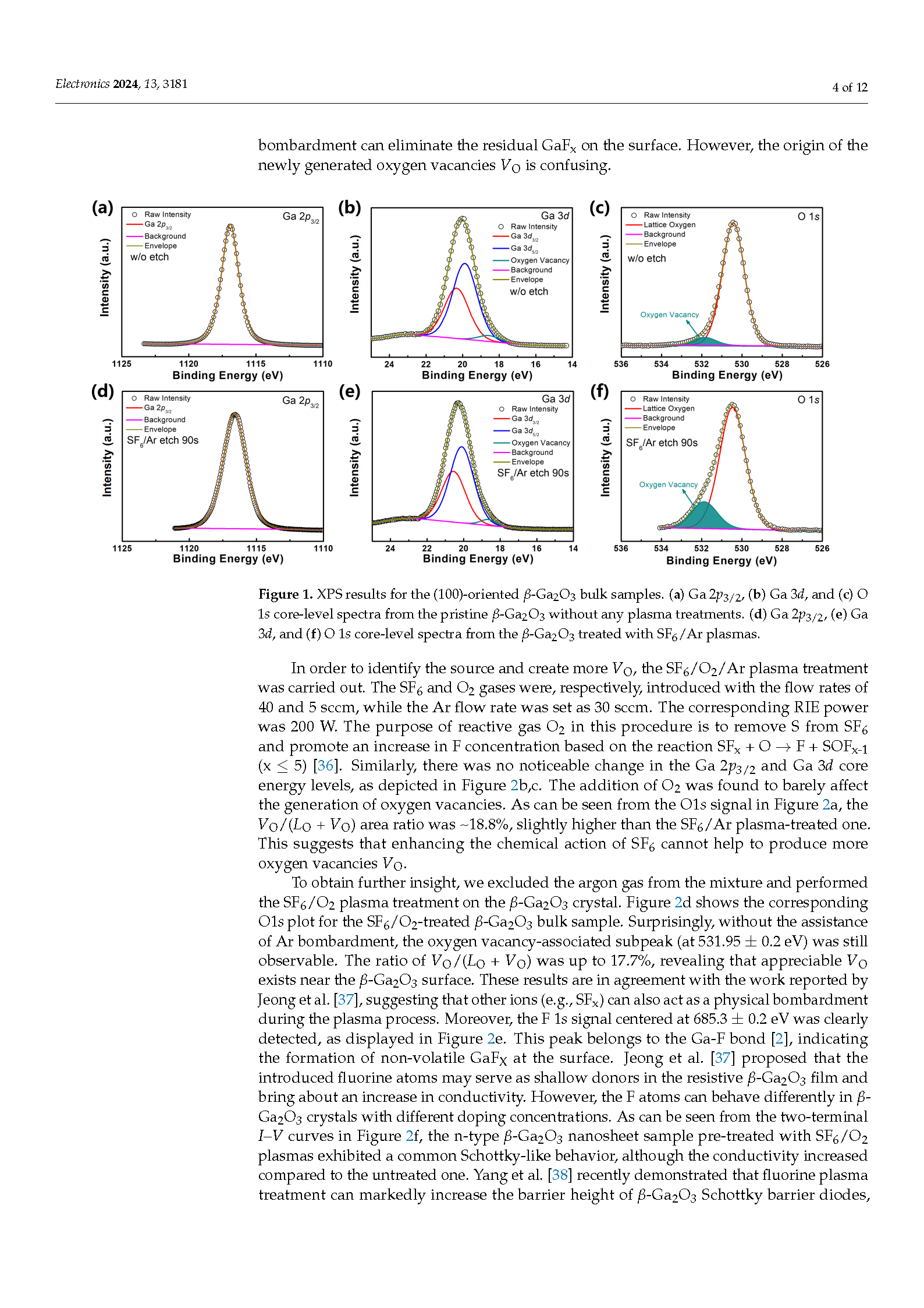
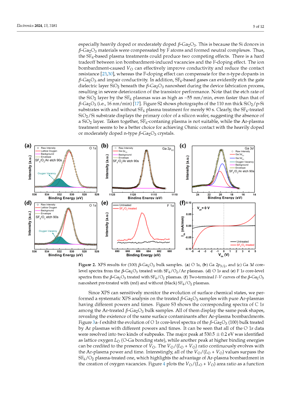
Figure 1. XPS results for the (100)-oriented β-Ga2O3 bulk samples. (a) Ga 2p3/2, (b) Ga 3d, and (c) O 1s core-level spectra from the pristine β-Ga2O3 without any plasma treatments. (d) Ga 2p3/2, (e) Ga 3d, and (f) O 1s core-level spectra from the β-Ga2O3 treated with SF6/Ar plasmas.
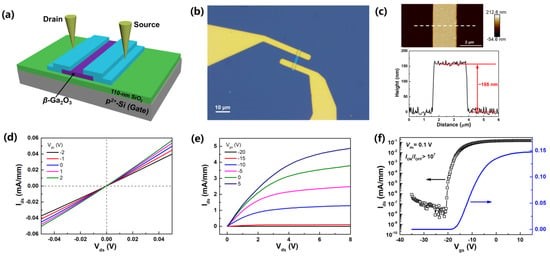
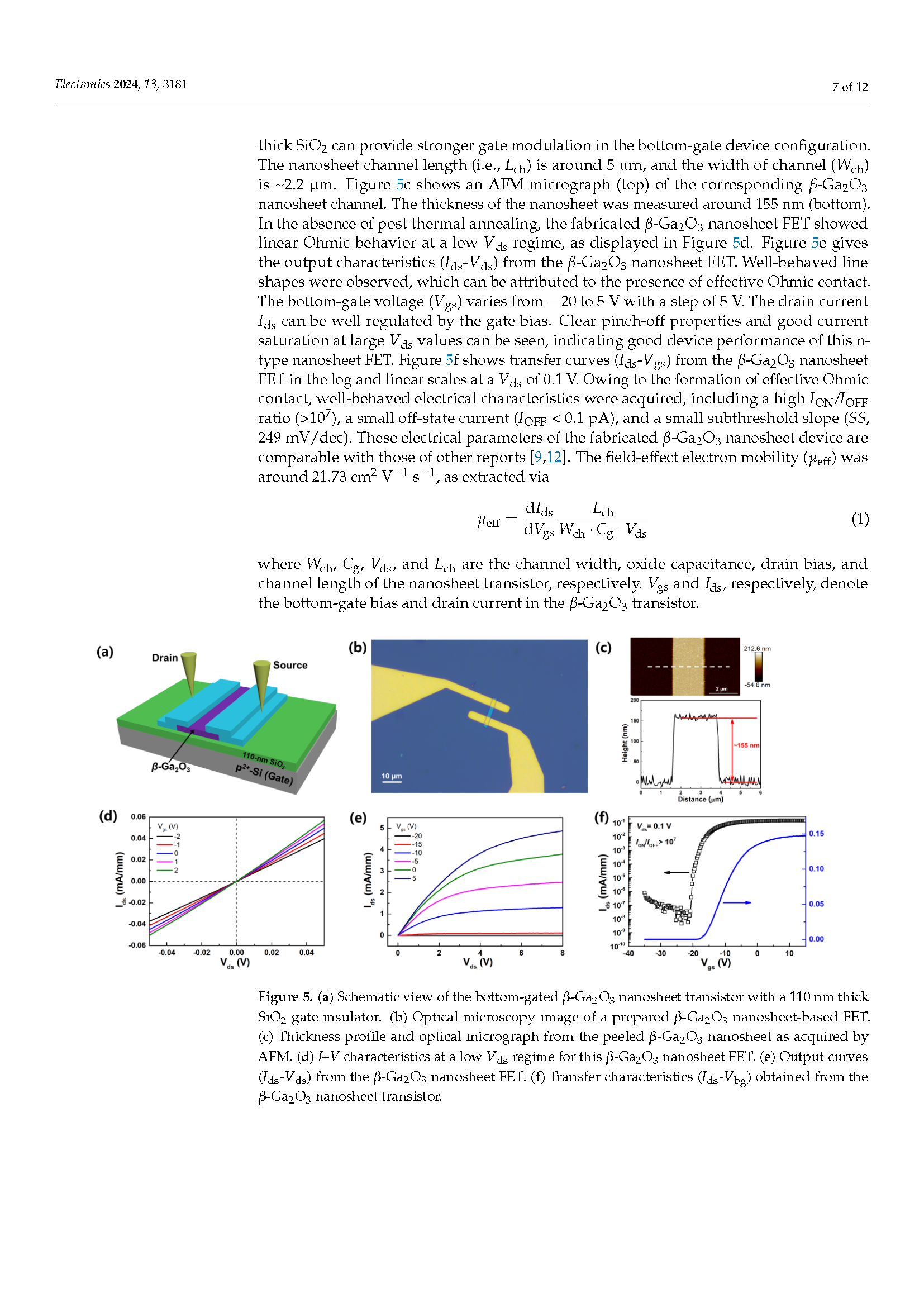
Figure 2. (a) Schematic view of the bottom-gated β-Ga2O3 nanosheet transistor with a 110 nm thick SiO2 gate insulator. (b) Optical microscopy image of a prepared β-Ga2O3 nanosheet-based FET. (c) Thickness profile and optical micrograph from the peeled β-Ga2O3 nanosheet as acquired by AFM. (d) I–V characteristics at a low Vds regime for this β-Ga2O3 nanosheet FET. (e) Output curves (Ids-Vds) from the β-Ga2O3 nanosheet FET. (f) Transfer characteristics (Ids-Vbg) obtained from the β-Ga2O3 nanosheet transistor.
DOI:
doi.org/10.3390/electronics13163181