


News Trends
【World Express】Prof. Masataka Higashiwaki Has been Selected as a Highly Cited Researcher 2024 at Clarivate 2024, Starting a New Journey in the Study of Gallium Oxide
日期:2024-12-04阅读:1059

On November 19, 2024, Clarivate Analytics released the list of Highly Cited Researchers for 2024. 6,836 scientists from over 1200 institutions in 59 countries and regions, totaling 6886 person-time, were selected to the list. The data shows that several papers ranked in the top 1% of cited times have had a significant academic impact on individual or multiple disciplines in both the natural and social sciences over the past decade.
Among them, in the field of Gallium Oxide research, Professor Masataka Higashiwaki from Osaka Metropolitan University in Japan was selected for the list. This is the third time that Professor Higashiwaki has been selected as a Highly Cited Researcher after 2021 and 2023.
Prof. Masataka Higashiwaki's Message:
We are very pleased that our research papers on Gallium Oxide devices have been widely cited, and we are honored to be selected as a "Highly Cited Researcher" for the third time. We believe this is a sign that research and development of Gallium Oxide is expanding globally. Thanks to the friends who have carried out joint research with me, I will be determined to continue to study the practical application of Gallium Oxide devices in the future.
The following is a review paper published recently by Professor Masataka Higashiwaki in the Annual Review of Materials Research named Beta-Gallium Oxide Material and Device Technologies.
ABSTRACT
Beta-Gallium Oxide (β-Ga2O3) is a material with a history of research and development spanning about 70 years; however, it has attracted little attention as a semiconductor for a long time. The situation has changed completely in the last ten years, and the world has seen increasing demand for active research and development of both materials and devices. Many of its distinctive physical properties are attributed to its very large bandgap energy of 4.5 eV. Another important feature is that it is possible to grow large bulk single crystals by melt growth. In this article, we first discuss the important physical properties of β-Ga2O3 for electronic device applications, followed by bulk melt growth and thin-film epitaxial growth technologies. Then, state-of-the-art β-Ga2O3 transistor and diode technologies are discussed.
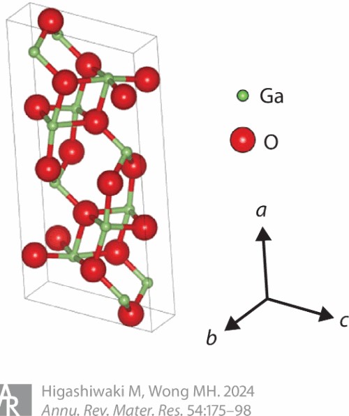
Figure 1. Atomic unit cell of β-Ga2O3.
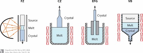
Figure 2. Ga2O3 melt growth methods. Abbreviations: CZ, Czochralski; EFG, edge-defined film-fed growth; FZ, floating zone; VB, vertical Bridgman.
For more information, please refer to the original link:https://doi.org/10.1146/annurev-matsci-080921-104058
