


Member News
【Member News】Research Progress and Technical Planning of Ultra-Wide Bandgap Semiconductor Technology by the Research Team of Shenzhen Pinghu Laboratory
日期:2024-12-13阅读:1601
Recently, Mr. Zhang Daohua of Shenzhen Pinghu Laboratory and Director Wan's team jointly sorted out an article on the research progress of Gallium Oxide P-type conduction, and was included in the special issue of “Gallium Oxide Materials and Devices” by Journal of Synthetic Crystal, which is expected to be officially launched next year.
In this paper, Ga2O3's research on materials and devices and their applications in power semiconductors have been summarized. The following is a summary of the content of the review articles.
Abstract: β phase gallium oxide (β-Ga2O3) is an ideal semiconductor material for power devices based on its ultra-wide bandgap, high breakdown electric field, and easy preparation. However, it is still challenging to realize p-type doping of the β-Ga2O3 because of its relatively low energy of valence band maximum (VBM) and flat band dispersion near the VBM, which limits the development of p-n junctions and bipolar transistors. The main strategies for the p-type doping of β-Ga2O3 in recent research are based on size effect, defect regulation, non-equilibrium dynamic process, and solid solution. For the β-Ga2O3 p-n homojunction and heterojunction, improving crystal quality and reducing the interface defect states are the key issues for optimizing devices’ performances. This paper systematically reviews the electronic structure of β-Ga2O3, the experimental characterization and theoretical calculation method of doping levels, the reasons for p-type doping difficulty, and the breakthrough in research advancements for improving the p-type doping of β-Ga2O3. Finally, the relevant studies on the β-Ga2O3 p-n homojunction and heterojunction devices are briefly reviewed. It requires further exploration to realize p-type doping of bulk-phase β-Ga2O3 through complex-defect regulation, non-equilibrium dynamics, solid solution, and combining these schemes. The device performances of p-n homojunction and heterojunction also need further optimization.
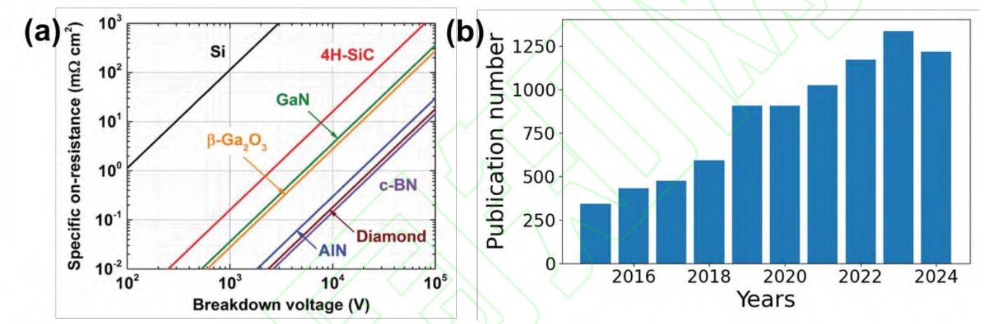
Fig. 1 Breakdown voltages and specific on-resistances for different semiconductor materials and the numbers of articles published on the Ga2O3 in the recent decade. (a) Relationship between the breakdown voltage and the specific on-resistance for Si,Ga2O3,GaN,SiC,AlN,BN, and diamond[4]; adapted with permission from Ref.[4]; (b) number of published articles on Ga2O3 in the recent decade. The source data are from the Web of Science (November 6, 2024)
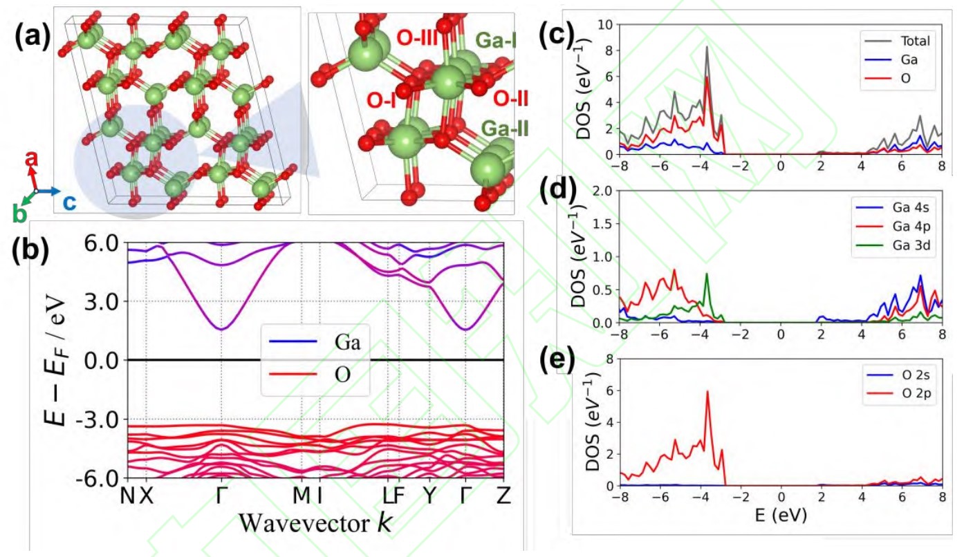
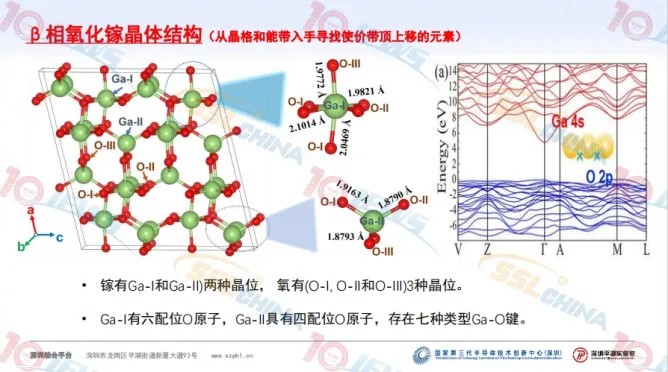
Fig.2 Crystal and electronic structures of β-Ga2O3. (a) 1×2×2 supercell of β-Ga2O3, the right part corresponds to the locally enlarged image[29], adapted from Ref. [29] under the copyright terms of Creative Commons CC BY Creative Commons; (b) band structure of β-Ga2O3; (c) element projected density of states of β-Ga2O3; (d) and (e) correspond to the orbital projected density of states of Ga and O in the β-Ga2O3
Academician Zhang Dao-hua: Research on Characteristics of Gallium Oxide and Aluminum Nitride in Ultra-Wide Bandgap Semiconductors
Ultra-wide bandgap semiconductors, including Gallium Oxide and Aluminum Nitride, have the characteristics of large bandgap, high breakdown electric field and power density, and strong anti-radiation ability, which have significant advantages in the application of extreme environments such as high temperature, high pressure and high radiation. At present, the challenges of ultra-wide bandgap semiconductors are mainly focused on the improvement of material properties, doping and defect regulation, and cost reduction.
Zhang Daohua
Chief scientist of the fourth-generation semiconductor of Shenzhen Pinghu Laboratory,
Academician of Singapore Academy of Engineering
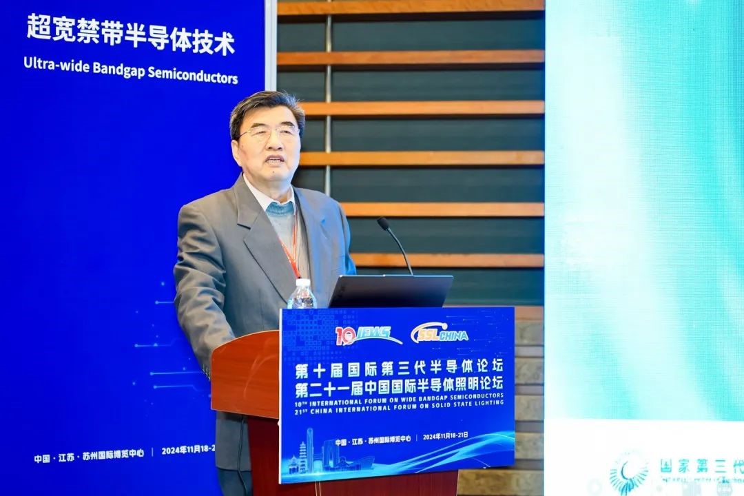
Recently, the 10th International Forum on Wide Bandgap Semiconductors & the 21st China International Forum on Solid State Lighting (IFWS&SSLCHINA2024) was held in Suzhou. During the session, on the "Ultra-Wide Bandgap Semiconductor Technology I" sub conference, Zhang Daohua, the fourth-generation semiconductor chief scientist of Shenzhen Pinghu Laboratory and Academician of Singapore Academy of Engineering, made a keynote report on "Research on Characteristics of Gallium Oxide and Aluminum Nitride in Ultra-Wide Bandgap Semiconductors ", discussing the research status and main problems of ultra-wide bandgap semiconductors. The recent theoretical research and material characterization of Gallium Oxide and Aluminum Nitride were shared. At the same time, the layout, planning, foundation and supporting facilities of Shenzhen Pinghu Laboratory in wide-band gap and ultra-wide-band gap semiconductor research were introduced, so as to facilitate the cooperation of colleagues and jointly promote the development of wide-band gap semiconductor science and technology.
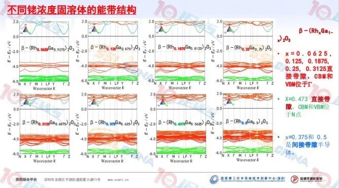
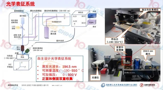
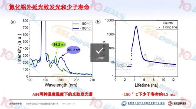
The report shared the research progress of Gallium Oxide and Aluminum Nitride. Related to the regulation of Gallium Oxide energy band structure, including β phase Gallium Oxide crystal structure, different metal positions in solid solutions, energy band structure of different metal solid solutions, average effective mass of holes in different metal solid solutions, crystal orientation distribution in rhodium solid solutions, and Aluminum Nitride/Aluminum-Rich Gallium Nitrogen photoluminescence measurements, Including optical characterization system, Aluminum Nitride epitaxial photoluminescence and minority carrier lifetime, and Aluminum-Gallium Nitride photoluminescence.

The report shows that Gallium Oxide faces the challenges of valence band flat, large hole mass, low hole mobility, difficult P-type doping of Gallium Oxide, and low thermal conductivity of β-Ga2O3. Most of the 49 metals replace the hexacoordination Ga-I atom more stable. The effective mass of most solid solution configurations decreased, and the value of β-(Rh0.25Ga0.75 ) 2O3 was 52.3% of that of β-Ga2O3. The top energy level of β-(RhxGa1-x) 2O3 valence band increases significantly in the range of 1.35~2.95 eV. Aluminum Nitride faces difficulty in controlling AlN doping, Si doping forms DX center, and the activation energy increases to 200 meV. Highly doped Si has a compensation effect, forming VAl + nSiAl, resulting in a decrease in electron concentration with the increase of Si doping; The activation energy of fitted Mg in AlN material is 630 meV; The high ohm contact resistance, the low AlN electronic affinity, leads to the challenges such as high specific contact resistivity.
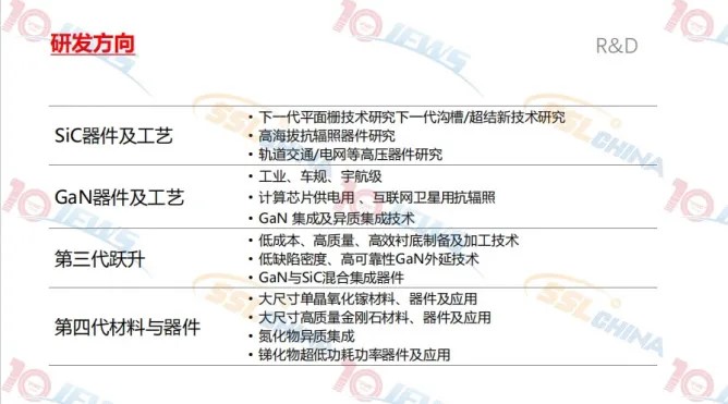
The research and development direction of Pinghu Laboratory involves SiC devices and processes, GaN devices and processes, the third-generation leap, the fourth-generation materials and devices, etc. The report points out that low-carbon, electrification and intelligence are the key elements to achieve Carbon Neutrality. The Industrial revolution was accompanied by the energy revolution, which accelerated the arrival of a green, low-carbon and smart world. Science and technology change the future, Shenzhen Pinghu Laboratory will build a bridge between research and industry, facing a variety of application prospects, and work together with partners to make breakthroughs and create a better future.
Guest Introduction
Zhang Daohua, former Chairman of Singapore Optoelectronics Association, member of Nanyang Technological University Competitive Research Project Review Committee, Professor of College of Power and Electronic Engineering, Director of Research Excellence Program Committee of College of Power and Electronic Engineering, Deputy Director of Department of Microelectronics, Deputy Director of Semiconductor Light-emitting Display Center, etc. He has presided over the completion of more than 30 research projects, including the first of its kind in Singapore and NTU's first S $10 million project, which was recognized as "Outstanding World-Class Research Progress" by a jury that included Nobel Prize winners. Zhang Daohua is currently the chief scientist of fourth-generation semiconductors at Shenzhen Pinghu Laboratory. He is a Fellow of the Physics Society (FInstP) and the Fellow of Institute of Engineering and Technology (FIET), and a Fellow of the Singapore Academy of Engineering (FSAEng).
About Pinghu Laboratory
In December 2021, National Center of Technology Innovation for Wide BandGap Semiconductors (Shenzhen) was authorized by the Ministry of Science and Technology. In August 2022, the Shenzhen Science and Technology Innovation Bureau held an event to establish the Shenzhen Pinghu Laboratory as the main operating unit. Focusing on SiC, GaN, next - generation advanced power electronic materials and devices, core equipment and components, and supporting materials, etc., and conducts research on core technologies.
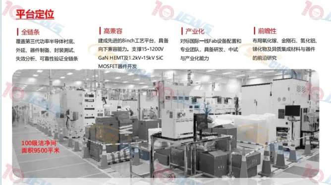
Shenzhen Pinghu laboratory located in Luoshan Science and Technology Park, Longgang District, Shenzhen, the laboratory covers an area of 130 mu, with a class100 clean room area of 9,500 square meters. It has the industry - leading wide - band - gap power semiconductor infrastructure and more than 380 sets of various advanced equipment from both international and domestic sources.
The laboratory has a staff scale of 350 people, gathering top talents from home and abroad, creating an open, public, and shared scientific research, pilot scale production, and analysis and detection platform for the whole country, and jointly building a sustainable future.
