


News Trends
【World Express】FLOSFIA, Announced Recent Plans and Technical Achievements for Ga₂O₃ Semiconductor Devices
日期:2024-12-19阅读:1881
FLOSFIA is committed to the development of Gallium Oxide (α-Ga2O3) semiconductor devices which is the world's most high-profile power semiconductor. To date, the company has achieved a number of groundbreaking results, including the world's first commercial-grade Schottky Barrier Diode (SBD) sample shipments under the GaO® brand, and has filed more than 700 α-Ga2O3 related patents
The following is an update on FLOSFIA's mass production and technology development plans.
Latest Mass Production Plan
The original plan was to mass produce FLOSFIA's initial product SBD, and 600V·10A samples have been sold. However, it has now been decided that the mass production schedule to start in 2024 will be adjusted.
In order to provide higher quality products, FLOSFIA hopes that relevant people can give some understanding and support.
FLOSFIA believe that more time is needed to stabilize all reliability assessments. In a small number of products in particular, the reliability issues detected primarily from the quality and stability deficiencies present in the surface processing of α-Ga2O3. FLOSFIA is actively taking steps to address these issues.
Latest Technology Development
FLOSFIA, on the other hand, has made steady progress in its technology development. In particular, the prototype of the Junction Barrier Schottky (JBS) structure diode using the new P-type semiconductor Iridium Gallium oxide α-(IrGa)O3, the realization of the normal turn-off operation of trench MOSFET, the expansion of wafer size, and other devices transformations of Gallium Oxide semiconductors. Innovative achievements have been made in Gallium Oxide semiconductor technology.
1.Successful Trial Production of New Generation SBD (JBS Structure) Sample
FLOSFIA has successfully trial-produced 600 V·10A product based on JBS structure (Figure 1). With this structure, the opening voltage is significantly improved from the original 1.4V to 0.9V, resulting in a significant increase in efficiency (Figure 2). In this trial production, α-(IrGa)2O3, the world's first P-type semiconductor material, was used, a result that is crucial for fully exploiting the high material potential of Gallium Oxide. It is planned to begin sample shipments and officially launch the product on the market in 2025.
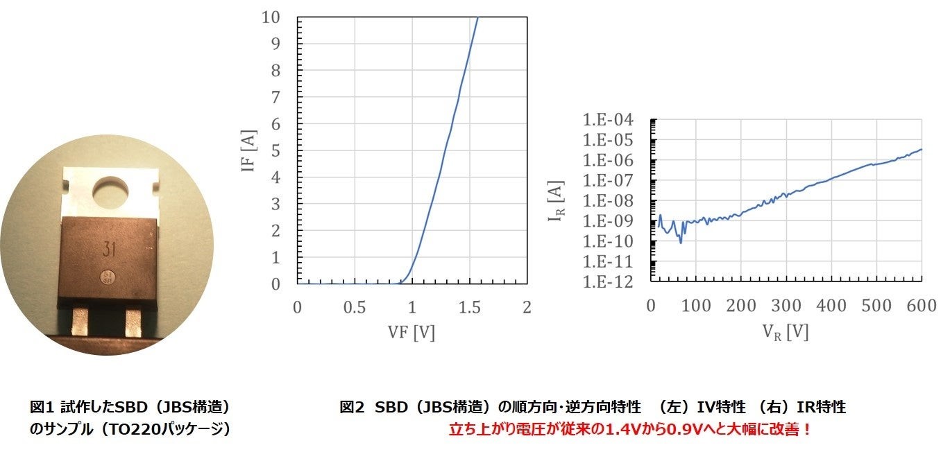
Figure 1. JBS structure SBD sample
Figure 2. Forward and reverse characteristics of SBD (JBS structure) (left) I-V characteristics (right) I-R characteristics
2.Operation Demonstration of Trench MOSFET Structure
Through process optimization and self-developed MOS interface control technology, FLOSFIA successfully verified the normally off operation of the trench MOSFET (Figure 3 · 4). FLOSFIA will make full use of the material potential of the new P-type semiconductor α-(IrGa)2O3 and continue to promote its mass production development.
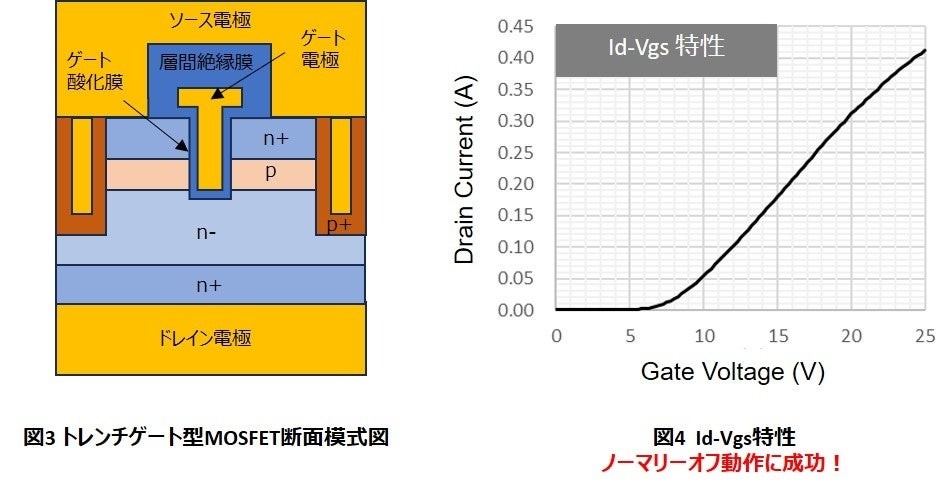
Figure 3. Working principle of trench MOSFET
Figure 4. Id-Vgs characteristic
3.Expansion of Wafer Size
In terms of α-Ga2O3 wafer development, FLOSFIA has realized the α-Ga2O3 epitaxial growth technology for 4-inch wafers, and the manufacturing technology for 3-inch wafers (Figure 5). We expect to complete the validation of the 4-inch wafer manufacturing technology in 2025. Large size will not only bring cost advantages, but also improve production efficiency. In addition, the Sapphire substrate used is the most widely used 4-inch specification in the market, and its price is only 1/10 to 1/50 of the Silicon Carbide (SiC) substrate of the same size, laying a solid foundation for achieving low cost in the future.
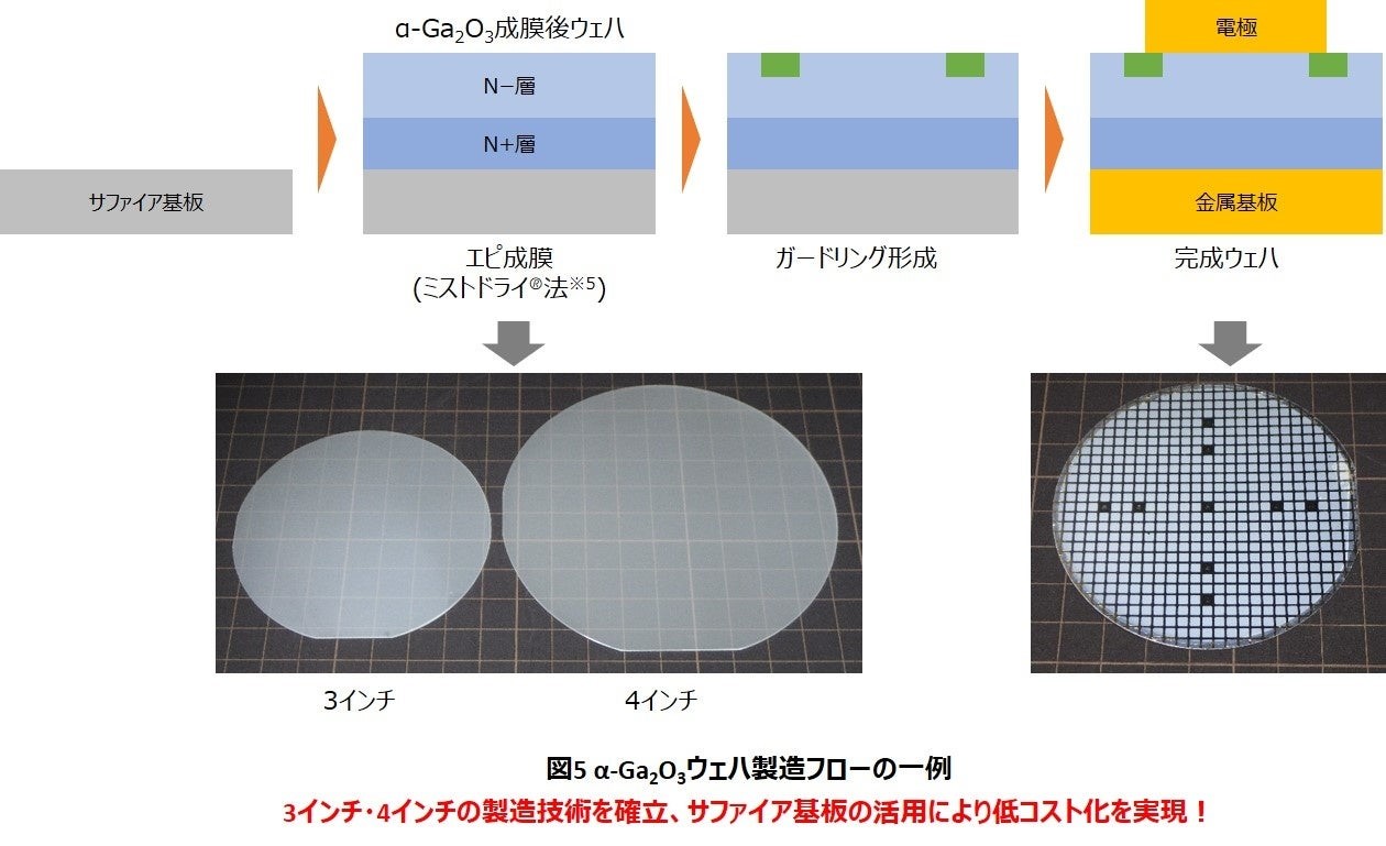
Figure 5. Example of α-Ga2O3 wafer manufacturing process
4.Establish the Basis for the Development of High-Voltage and High-Current Devices
FLOSFIA plans to expand the voltage level of the device to 600 V, 1200 V, 1700 V, and the current specification from 10A to hundreds of A levels. The underlying technology has been developed and the next step will be to accelerate the productization process.
Establish Partnership for Mass Production and Future Outlook
Based on the above technology development results, FLOSFIA plans to build a sound mass production system and actively seek partners. By providing intellectual property licensing, epitaxial wafer supply and other means, FLOSFIA will establish closer cooperation with enterprises.
Believing in the transformative potential of Ga2O3 semiconductor devices, FLOSFIA will continue to advance technology development and market expansion as an industry leader. Through the new partnership, FLOSFIA will achieve high performance, high reliability of Ga2O3 semiconductor device mass production, while optimizing losses of material including rare substances, manufacturing and material process, advancing the goal of "Semiconductor Ecology ®."
