


News Trends
【World Express】Gallium Oxide Heterojunction Diode Demonstrates Avalanche and Surge Robustness
日期:2024-12-31阅读:1554
Amongst the ultrawide-bandgap (UWBG) semiconductor materials, the beta phase of gallium oxide (ß-Ga2O3) is perhaps the most promising. Significant progress has been demonstrated on high-voltage MOSFET and MESFET devices. The use of a nickel oxide (NiO) p-layer has allowed for the creation of heterojunction diodes (HJDs). In this article, we summarize work done on ß-Ga2O3-NiO HJDs that showcases excellent avalanche and surge performance in these devices, making them potential candidates for use in future high-voltage power systems.
HJD fabrication
Two-inch tin-doped (001) ß-Ga2O3 substrates were the starting point for the device fabrication. The drift region comprises a 10-µm-thick silicon-doped n-Ga2O3 layer with a carrier concentration of ~1.7 × 10¹⁶/cm3. The epi wafers are commercially available from Novel Crystal Technology (Japan). A tin/gold (Ti/Au) metallization and annealing is done to form the cathode on the back of the thinned wafer. A double layer of NiO is deposited above the drift layer using RF magnetron sputtering. This forms the anode layer and creates the heterojunction to the n-Ga2O3. The base NiO layer is p–, with a hole concentration of 5.8 × 10¹⁷/cm3, while the upper p+ NiO has a hole concentration of 2.9 × 10¹⁹/cm3. The doping is varied by tuning the flux ratio of argon (Ar)/O2 in the sputtering process. A small-angle (11°) beveled edge was created in the NiO to create a junction-termination-extension edge termination. This bevel is created by combining a shadow mask at a certain distance from the wafer and a declination angle of the NiO target to the wafer, both adjustable parameters. A gradual decrease in the surface electric field is thus achieved away from the device’s active region. A barium titanate perovskite oxide (BaTiO3) is also deposited by RF sputtering on top of the NiO film. This has an ultrahigh dielectric constant and forms a field plate under the anode metal (Ni/Au), which extends past the NiO layer. With the use of this field plate, the peak electric field in the Ga2O3 and NiO is lowered from 6.61 MV/cm and 7.91 MV/cm to 4.57 MV/cm and 2.62 MV/cm, respectively.
The 3 × 3-mm device cathode was bonded onto a 0.5-mm-thick copper-molybdenum-copper substrate with high thermal conductivity, while the anode was connected to the lead frame by five 1-mm-thick Au bond wires. Encapsulation and mounting onto TO-220 packages completed the fabrication process. A simplified layer schematic of the device is shown in Figure 1.

Figure 1: Layer schematic of the HJD (Source: Zhou et al., 2023)
Avalanche performance
Avalanche behavior can be an important robustness factor in a power semiconductor, especially in motor drive applications in which turn-off back-EMF produced from inductive loads needs to be dissipated. The p-n junction can create impact ionization and multiplication once the reverse voltage across the device reaches the avalanche breakdown (BAVA). A high reverse current flow (IAVA) is enabled, allowing avalanche energy (EAVA = BAVA × IAVA × time duration of event) to be dissipated without causing catastrophic device failure. An unclamped inductive switching (UIS) test is typically done to test the avalanche robustness of the device. In the UIS test, an inductor is charged through a switch, which when turned off forces the energy stored in the inductor through the off-state device under test (DUT), causing it to enter avalanche breakdown. The ability of the DUT to withstand a repeated UIS test without a significant change in its forward or reverse characteristics gives further confidence in its avalanche robustness.
The HJD device’s UIS performance is shown in Figure 2. The BAVA ranges from 1,545 V to 1,683 V across temperatures from 25°C to 175°C, with a positive temperature coefficient of 1 V/°C. The reverse characteristics in Figure 2a show leakage current at 1,200 V of 100× to 1,000× lower than that of a similarly rated SiC merged PiN Schottky diode, demonstrating the advantages of the UWBG technology. The test setup is shown in Figure 2b and the UIS waveforms in 2c. The HJD passes 1 million repeated UIS tests at an IAVA of 30 A and a BAVA of 1,740 V for a 20-µs duration. The forward and reverse characteristics showed no significant change after this test compared with a fresh part. The stable avalanche performance is attributed to the impact ionization starting in the n-Ga2O3 region and proceeding uniformly through the entire device. The staggered band structure of the heterojunction does not create a barrier of holes at a high reverse bias, allowing efficient hole removal.
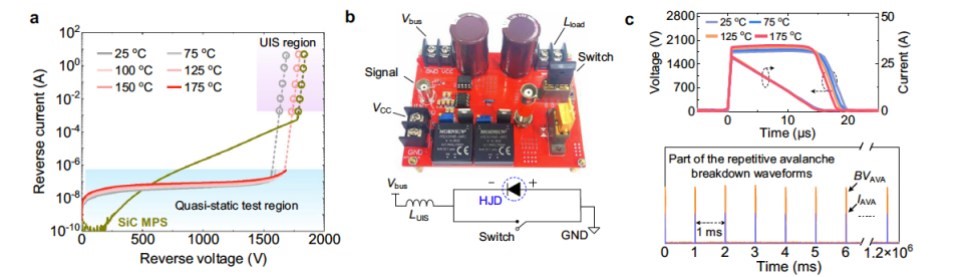
Figure 2: (a) The quasistatic reverse characteristics of the HJD versus temperature, indicating the UIS region for avalanche testing; (b) the UIS test circuit; (c) the UIS waveforms at 30 A, 20 µs and the HJD passing 1 million repeat UIS tests (Source: Zhou et al., 2023)
Surge performance and reverse recovery
This tests the device’s robustness at a high forward-conduction state. A 10-ms half-sinusoidal current pulse with an adjustable amplitude is used. As shown in Figure 3, the HJD can withstand a 50-A surge.
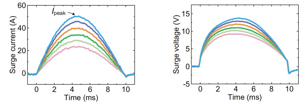
Figure 3: Surge current and voltage characteristics of the HJD (Source: Zhou et al., 2023)
It exhibits a negative temperature coefficient of the on-resistance (RON), suggesting bipolar conductivity modulation. In a homojunction p-n diode, the lightly doped drift region accumulates minority carriers, leading to a considerable reverse recovery when the device is switched off. This causes increased switching loss and limits switching speed. Hence, an inherent tradeoff exists in homojunction p-n devices between surge robustness and switching speed.
The reverse-recovery characteristics of the HJD device are shown in Figure 4. Unlike the curves of the fast silicon p-n diode shown here for comparison, the reverse-recovery waveforms of the HJD are independent of the forward current and exhibit very fast recovery. The reverse-recovery time of this HJD has been extracted to be 12.79 ns. The high-surge capability is attributed to electron injection into the NiO via tunneling or thermionic emission at high forward biases. Under reverse bias, the depletion occurs mainly in the lightly doped n-Ga2O3 region with minimal minority recombination in the NiO. A low hole minority carrier lifetime of 6.2 ns in Ga2O3 is extracted from electron-beam-induced-current studies. The theoretical conclusions based on the measurements suggest that under surge conditions, a high electron concentration is present in the entire NiO region, resulting in conductivity modulation, while the hole concentration in Ga2O3 is much lower and drops rapidly away from the junction.
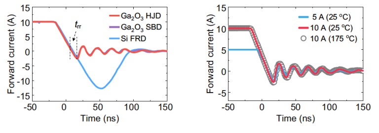
Figure 4: Reverse-recovery characteristics of the HJD (Source: Zhou et al., 2023)
The NiO/Ga2O3 heterojunction can be a promising material system for creating robust power devices. The HJD device summarized here shows good surge and avalanche performance with advantageous tradeoffs between the RON and breakdown voltage characteristics. This heterojunction has also been used to create superjunction MOSFET devices by other groups. Further advances in this technology can push these devices toward their theoretical limits and make them appealing for use in high-voltage power systems.
