


Member News
【Member News】Hangzhou GAREN SEMI Made a Breakthrough in Gallium Oxide Substrate Technology to Help Customers Achieve 2400V Enhanced Transistor
日期:2024-12-31阅读:1292
In December 2024, Hangzhou GAREN SEMI Co., LTD. (hereinafter referred to as "GAREN SEMI") made a major breakthrough in the field of ultra-wide bandgap semiconductor materials. The company worked with downstream customers to conduct in-depth device validation on GAREN SEMI (010) surface Gallium Oxide semi-insulating substrates. The enhanced transistor with excellent performance was successfully prepared, with a breakdown voltage of up to 2429V, and the performance index was significantly improved compared with the device verification results of the imported substrate. This achievement not only shows the leading position of GAREN SEMI in Gallium Oxide substrate technology, but also lays a solid foundation for the mass production application of domestic Gallium Oxide substrate in power devices.
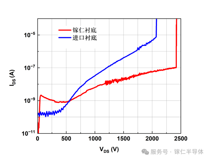
Breakdown Curve
Leading Performance Parameter
Among the main crystal faces of Gallium Oxide single crystal substrates, the (010) crystal face has unique physical properties, which make it have excellent performance in epitaxy and devices. First of all, the (010) substrate has the highest thermal conductivity, which is conducive to enhancing the device heat dissipation and improving the performance of power devices; Secondly, (010) substrate has a fast epitaxy growth rate, improving epitaxy efficiency.
Based on the (010) surface Gallium Oxide semi-insulated substrate provided by GAREN SEMI, downstream device customers have realized enhanced transistors with on/off ratio greater than 107, breakdown voltage up to 2429V, device gate drain distance 30 μm, gate width 3 μm, and off-state leakage ~10-7mA/mm. Under the same conditions, the device performance of the GAREN substrate is significantly better than that of the imported substrate (2080V).
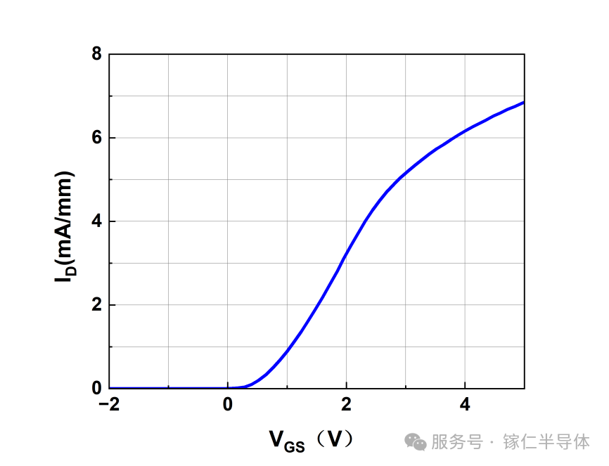
Transfer Characteristic Curve
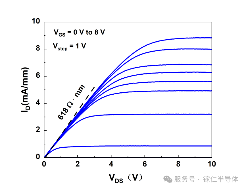
Output Curve
Technological Innovation and Industrial Breakthrough
This progress of GAREN SEMI is due to its continuous innovation in Gallium Oxide single crystal growth technology.
In March 2024, the company successfully prepared 6-inch high-quality Gallium Oxide single crystal substrate using the casting method independently created by Academician Yang Deren's team.
In April 2024, GAREN SEMI launched a 2-inch wafer-scale (010) Gallium Oxide semi-insulated single crystal substrate and achieved independent mass production, becoming the world's only wafer-scale (010) Gallium Oxide substrate supplier.
In September 2024, the company launched the first domestic Gallium Oxide special VB method crystal growth equipment, filling the domestic technology gap and further helping the development of domestic Gallium Oxide material industry.
New Advantages in International Competition
Faced with the increasingly severe international situation, especially the challenge of the embargo policy of Gallium Oxide materials, the technological breakthrough of GAREN SEMI is particularly important. The device performance achieved by downstream customers on the GAREN SEMI substrate exceeds that of imported products, which further proves the competitiveness of GAREN SEMI material technology. The company's innovation achievements not only help the domestic industry break the international monopoly, but also promote the high-quality development of the industry.
Summary and Outlook
This technological breakthrough of Hangzhou GAREN SEMI Co., Ltd. not only shows China's strong strength in the field of fourth-generation semiconductor materials, but also contributes Chinese wisdom to the development of the global semiconductor industry. With the continuous progress of technology and the acceleration of industrial application, GAREN SEMI is expected to play a more important role in the future semiconductor industry.
Company Profile
Hangzhou GAREN SEMI Co., Ltd. was established in September 2022, is a technology enterprise focusing on the research and development, production and sales of Gallium Oxide and other semiconductor materials. The company has created a new technology for Gallium Oxide single crystal growth, and has more than ten international and domestic invention patents, breaking through the monopoly and blockade of Western countries such as the United States and Japan on Gallium Oxide substrate materials. Based on solving the major national needs, GAREN SEMI will be deeply engaged in the continuous innovation of the Gallium Oxide upstream industry chain, and strive to provide product guarantee for the development of China's power electronics and other industries.
For more information about GAREN SEMI and its products
Please visit our official website: http://garen.cc/
Or contact us:
Mr. Jiang :15918719807
Email: jiangjiwei@garen.cc
Mr. Xia :19011278792
Email:xianing@garen.cc
