


News Trends
【World Express】FURI Project Supports College Research to Improve Wide Bandgap Semiconductor sustainability
日期:2025-01-06阅读:1223
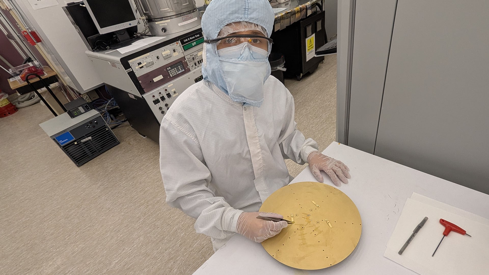
David McComas, an undergraduate electrical engineering student in the Ira A. Fulton Schools of Engineering at Arizona State University, deposits a metal mask on a gallium oxide wafer in the ASU NanoFab semiconductor fabrication facility. McComas is working on a Fulton Undergraduate Research Initiative, or FURI, project to improve microelectronics sustainability, one of eight FURI projects sponsored by semiconductor manufacturer TSMC in the fall semester. Photo courtesy of David McComas
As microelectronics have become an increasingly essential part of modern society, greenhouse gas emissions, which are associated with their use and manufacture, have increased in tandem. Semiconductor manufacturing contributes 31% of greenhouse gas emissions worldwide, and a U.S. Department of Energy analysis of data from the Intergovernmental Panel on Climate Change estimates greenhouse gas emissions associated with semiconductors could quadruple by 2030.
Research efforts are underway to reduce the essential field’s environmental impact by a team of students in the Ira A. Fulton Schools of Engineering at Arizona State University, who are exploring ways to make microelectronics manufacturing more eco-friendly. Their research is sponsored by TSMC, one of the world’s largest microelectronics manufacturers with an increasing presence as part of the semiconductor industry’s rapid expansion in Arizona.
Undergraduate students in the Fulton Undergraduate Research Initiative, known as FURI, work under faculty members to apply knowledge gained in the classroom through hands-on research experience. TSMC funded eight FURI projects related to semiconductor manufacturing in the fall 2024 semester, some of which focused on increasing the sustainable use and manufacturing of semiconductors.
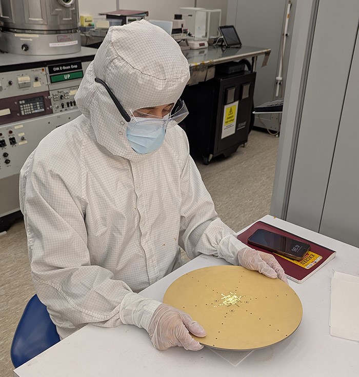
David McComas works with gallium oxide, a type of semiconductor material, in the ASU NanoFab. Photo courtesy of David McComas
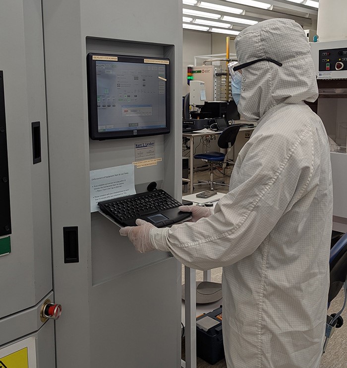
David McComas works with equipment in the ASU NanoFab. Photo courtesy of David McComas
Reducing electronics manufacturing emissions at the source
Fulton Schools chemical engineering undergraduate student Jay Schroeder decided to focus his sponsored FURI project on a different aspect of sustainability related to semiconductors: reducing the production of greenhouse gas emissions during manufacturing.
Under the supervision of Shuguang Deng, a Fulton Schools professor of chemical engineering, Schroeder is exploring the efficacy of porous, crystalline materials known as zeolites at adsorbing a gas called tetrafluoromethane, which is used during the etching process in semiconductor manufacturing. Etching is when parts of semiconductor material are removed to allow for the placement of other components later in the manufacturing process.
Tetrafluoromethane is a greenhouse gas that causes approximately 6,500 times as much atmospheric warming as carbon dioxide. Current semiconductor manufacturing methods capture the gas via cryogenic distillation, where the gas is compressed and frozen to ensure it doesn’t escape into the air.
The process doesn’t capture all emitted tetrafluoromethane, and it requires high amounts of energy to do so. In contrast, zeolite materials can bind the gas molecules to them with little to no electricity needed while leaving a smaller amount of tetrafluoromethane uncaptured, if any escapes at all.
“The gas would just have to pass over the surface, with or without electricity, and the surface would bond to the tetrafluoromethane, removing it from the air and holding it on the zeolite surface, much like how exhaust passes through a catalytic converter on a car,” Schroeder says.
He is exploring the predicted efficacy of different zeolite materials using density functional theory, which calculates the expected yet unconfirmed properties of materials. Schroeder uses the theory to narrow down which zeolite materials are likely to perform well for tetrafluoromethane capture, then simulates the expected performance through Grand Canonical Monte Carlo methodology to more accurately predict zeolite behavior.
After Schroeder completes his portion of the project by running simulations, Deng will use the results to determine which zeolite materials to physically test with graduate students in a lab setting under a variety of conditions.
Building a future of more ecologically friendly electronics
Deng says sponsorship from TSMC has enabled an increased number of research opportunities.
“TSMC’s commitment to supporting sustainability-oriented research at the undergraduate level is truly commendable,” he says. “This funding not only advances semiconductor sustainability, but also strengthens the broader science, technology, engineering and math ecosystem by investing in young researchers poised to drive future innovations.”
As a FURI project mentor, Deng encourages undergraduate students to get involved in semiconductor research through the program.
“Projects like these provide technical experience and help students understand the importance of sustainable practices in technology-driven industries,” he says. “Working on industry-backed research also provides valuable insight into potential career paths and strengthens problem-solving skills that are highly sought after in the semiconductor sector.”
