


News Trends
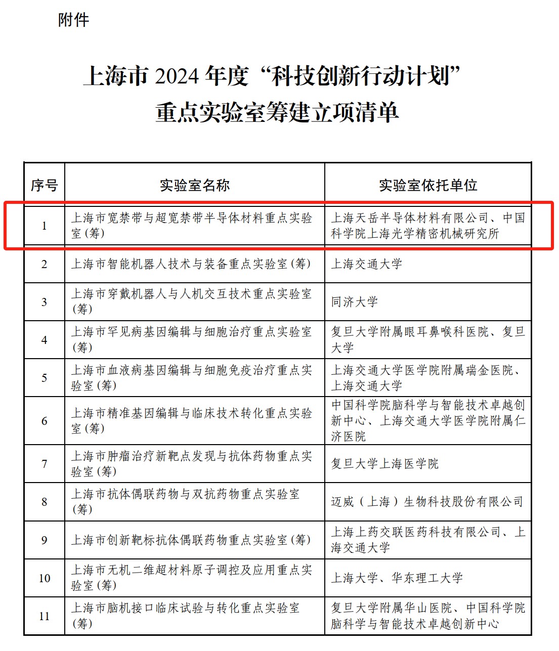
【Domestic News】Research Advancement of Gallium Oxide Materials -- Establishing Shanghai Key Laboratory of Wide Bandgap and Ultra-Wide Bandgap Semiconductor Materials
日期:2025-01-08阅读:1652
Science-and-Technology-Commission-of-Shanghai-Municipality on December 31 issued a notice on the preparation of the key laboratory of Shanghai 2024 "Science and Technology Innovation Action Plan". According to the "Shanghai 2024 ‘Science and Technology Innovation Action Plan’ Key Laboratory (First Batch) Application Guide "and" Measures for the Construction and Operation Management of Shanghai Key Laboratories "( Science-and-Technology-Commission-of-Shanghai-Municipality Regulation (2022) No. 6) relevant provisions, together with the recommendation departments to review and demonstrate, The establishment of 11 key laboratories, including Shanghai Key Laboratory of Wide Bandgap and Ultra-Wide Bandgap Semiconductor Materials, has been initiated.
Shanghai is actively promoting the construction of Shanghai Global Scientific and Technological Innovation Center, focusing on the field of semiconductor integrated circuits, and accelerating the construction of wide bandgap and ultra-wide bandgap semiconductor industrial systems.
Among them, the ultra-wide bandgap semiconducting material, Gallium Oxide, has become a national strategic material because of its significant advantages such as wide bandgap, high breakdown field strength and strong radiation resistance. At present, Gallium Oxide single crystal technology has reached the 6-inch level required for device industrialization, and single crystal growth equipment has the ability of "AI One-Key Crystal Growth". MOCVD technology also shows obvious advantages in batch preparation of Gallium Oxide homogeneous epitaxial films, and the performance of Gallium Oxide devices has exceeded the theoretical limit of Silicon Carbide. However, compared with the industrialization level of wide band gap semiconductor materials, Gallium Oxide materials and devices are still in the stage of industrialization cultivation, and there are problems such as insufficient basic theoretical mechanism support, immature industrial technology, and imperfect industry-education-research system and mechanism. These bottlenecks restrict the further development of the industry to a certain extent.
Shanghai Tianyue Semiconductor Materials Co., LTD. (hereinafter referred to as: Shanghai Tianyue) and Shanghai Institute of Optics and Fine Mechanics, Chinese Academy of Sciences (hereinafter referred to as: Shanghai Institute of Optics and Fine Mechanics) jointly established the " Shanghai Key Laboratory of Wide Bandgap and Ultra-Wide Bandgap Semiconductor Materials". Qi Hongji Researcher of Shanghai Institute of Optics and Fine Mechanics is co-executive director of the laboratory. He mainly conducts basic theoretical research and application research on the preparation of Gallium Oxide and Diamond crystals, focusing on the efficient preparation technology of large-size, low-cost, extremely low dislocation density and ultra-wide bandgap semiconductor materials. Shanghai Key Laboratory of Wide Bandgap and Ultra-Wide Bandgap Semiconductor Materials takes industrialization as the goal orientation, promotes the deep integration of technological research innovation and applied research innovation, and cultivates new quality productivity; support Shanghai to become China's wide bandgap and ultra-wide bandgap semiconductor innovation highland, forming an industrial innovation cluster with global influence.
Introduction of Shanghai Institute of Optics and Fine Mechanics
Shanghai Institute of Optics and Fine Mechanics is one of the earliest research units of Gallium Oxide crystal in China. In 2017, it launched the first Cross-Strait Conference on Gallium Oxide. The Gallium Oxide project team has undertaken a number of national and regional projects related to Gallium Oxide crystal, including: National Key Research and Development Program of China, Special Project of the Ministry of Industry and Information Technology of China, Shanghai Strategic Frontier Special Project and a number of The National Natural Science Foundation of China. In addition, focusing on the development needs of local industrial transformation and upgrading, they actively promote the transformation of scientific and technological achievements, forming a pattern of scientific and technological innovation and transformation with Shanghai Institute of Optics and Fine Mechanics as the source of scientific and technological innovation and transformation platform as the pilot incubation base of achievements. Relying on the achievement transformation platform of Hangzhou Institute of Optics and Fine Mechanics, Gallium Oxide team founded Hangzhou Fujia Gallium Technology Co., Ltd. in 2019, committed to transforming scientific research achievements into actual productivity and promoting the large-scale application and industrialization of Gallium Oxide materials. Since its establishment, the company has carried out a "single crystal - epitaxy - device" full chain layout around Gallium Oxide technology, and strives to occupy a leading position in the field of ultra-wide bandgap semiconductors.
