


Member News
【Member News】Fujia Gallium Cooperation Research Achievements Listed in Materials Today Physics, High-Quality MBE Epitaxial Film Performance Comparable to the Highest International Technical Level
日期:2025-01-13阅读:1583
Under the support of National Key Research and Development Program "Research on Large-Size Gallium Oxide Semiconductor Materials and High-Performance Devices" (Project Number: 2022YFB3605500), Zhang Hongliang from Xiamen University systematically studied the electrical transport properties of Gallium Oxide thin films prepared by Molecular Beam Epitaxy (MBE) provided by Hangzhou Fujia Gallium Industry Technology Co., LTD. (hereinafter referred to as: Fujia Gallium), and are compared with those of Japanese and American research teams. The results show that the electrical properties of Gallium Oxide MBE epitaxial wafer grown by Fujia Gallium are equivalent to the highest level abroad. In addition, in collaboration with a team from the Shanghai Institute of Optics and Fine Mechanics, Chinese Academy of Sciences, the activation mechanism of Sn doping and the microscopic information of the defect state were studied by combining the variable temperature electrical transport properties and high-resolution photoelectron spectroscopy, providing guidance for further optimization of doping strategies and device performance. The results of the study were published in Materials Today Physics (Impact Factor 10.0).
Gallium Oxide is a newly emerging ultra-wide bandgap semiconductor material with excellent material properties such as ultra-wide bandgap, ultra-high voltage and high thermal stability. It is the preferred material for a new generation of power electronic devices and deep ultraviolet optoelectronic components, and has potential applications in high-end fields such as new energy vehicles, rail transit, smart grid, aerospace and missile warning. Gallium Oxide is therefore known as the "fourth generation" semiconductor. Gallium Oxide materials and devices are therefore highly valued by the semiconductor industry and academia around the world, and are developing rapidly. In August 2022, the United States and Japan successively imposed an embargo on Gallium Oxide on China, highlighting its importance in international strategic competition. The industrial chain of Gallium Oxide semiconductors includes single crystal substrate, thin film epitaxy and device fabrication. Among them, the epitaxial film is the key link connecting the Gallium Oxide substrate and the device, and its quality determines the device performance. In order to realize high-performance Gallium Oxide electronic devices, it is necessary to prepare epitaxial films with low defect density and high mobility, and precisely regulate their electrical properties. MBE technology can achieve precise control at the atomic level during thin film growth, and can obtain thin films with low defect density and extremely high interface quality. These advantages are of great significance for lateral devices or high electron mobility transistors (HEMTs) constructed by interfacial two-dimensional electron gas.
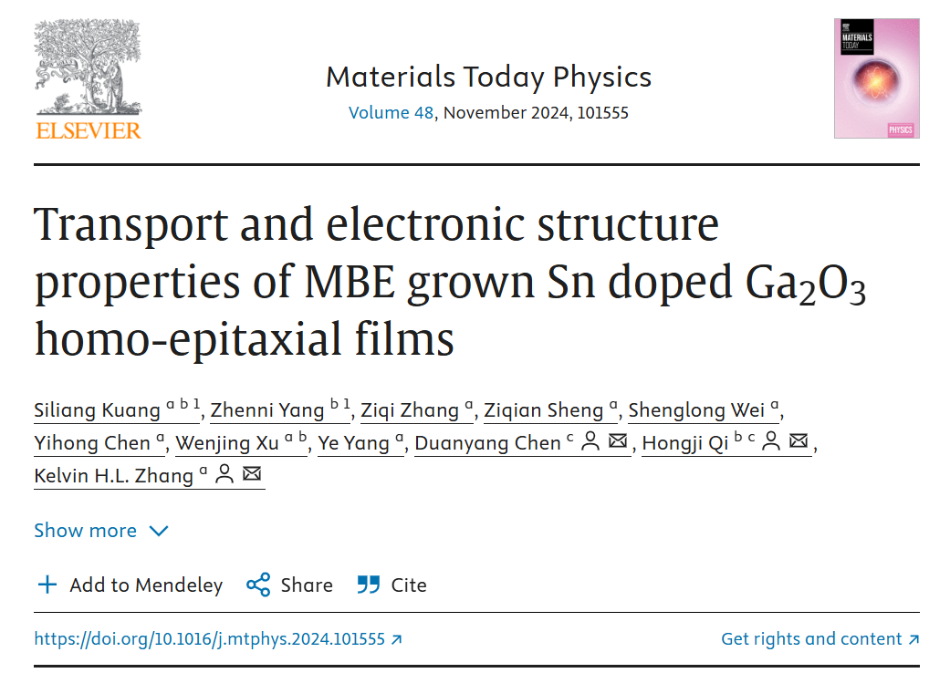
Fujia Gallium is one of the first units to develop MBE epitaxy Gallium Oxide thin films in China, and successfully grow Unintentionally Doped (UID) Ga2O3 thin films by MBE technology. The background carrier concentration can be controlled at 1.6×1016 cm-3, and the electron mobility at room temperature can be as high as 129 cm2V-1s-1. On this basis, Ga2O3 films with different Sn doping concentrations were further prepared by precisely adjusting the temperature of the K-cell of the Sn doping source, and the carrier concentration could be controlled from 1.7×1017 cm-3 to 2.8×1019 cm-3 in a wide range (FIG. 1a). The electrical properties of Sn-doped Gallium Oxide MBE epitaxy films are comparable to the highest levels achieved by NCT (novel crystal technology) in Japan and Professor James Speck's team at the University of California, Santa Barbara (UCSB) in the United States using MBE technology (Figure 1b).
Figure 1. (a) Carrier concentration and mobility of Ga2O3 thin films obtained at different Sn source temperatures; (b) This work is compared with other reports on the migration-carrier concentration relationship of Ga2O3 thin films grown by MBE.
On this basis, the research team combined with the variable temperature transport test and the internationally advanced synchrotron radiation hard X-ray photoelectron spectroscopy (British Diamond Light Source) to systematically study the electrical transport properties and electronic structures of the epitaxial thin films. The study revealed the evolution laws and physical mechanisms of micro information such as the electrical transport mechanism, defect states, and electronic structure of Sn doped Ga2O3 thin films with Sn doping.
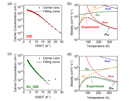
FIG. 2 Experimental data and fitting results of variable temperature (a) carrier concentration and (b) mobility of UID Ga2O3; Experimental data and fitting results of variable temperature (c) carrier concentration and (d) mobility of Sn doped Ga2O3.
The relevant work was published in Today Physics 48, 101555 (2024). with the title " Transport and electronic structure properties of MBE grown Sn doped Ga2O3 homo-epitaxial films"
Links to Articles:
Transport and electronic structure properties of MBE grown Sn doped Ga2O3 homo-epitaxial films
Materials Today Physics 48, 101555 (2024)
https://www.sciencedirect.com/science/article/pii/S2542529324002311
About Fujia Gallium
Hangzhou Fujia Gallium Technology Co., LTD., founded on December 31, 2019, is the first "hard technology" enterprise registered by Hangzhou Institute of Optics and Fine Mechanics. With the vision of "Making the World Use Good Materials", the company focuses on the industrialization work of wide bandgap semiconductor Gallium Oxide materials. Mainly engaged in the growth of Gallium Oxide single crystal materials, Gallium Oxide substrate and epitaxial wafer research and development, production and sales, the products are mainly used in power devices, microwave radio frequency and photoelectric detection fields.
At present, the company has won a number of honors: In 2022, it won the Zhejiang Province Science and Technology Small and Medium-Sized Enterprise; National High-Tech Enterprise in 2023; In 2024, it will be awarded as Hangzhou Enterprise High-Tech Research and Development Center and Zhejiang Special Small and Medium-Sized Enterprise. It undertook one Gallium Oxide project for the National Development and Reform Commission and participated in three national and provincial projects from the Ministry of Science and Technology, Zhejiang Province, and Shanghai. In addition, it has obtained 12 international patents authorized (6 in the United States and 6 in Japan), 40 domestic patents authorized, 3 trademark certification and registration of "Fujia Gallium Industry", and 3 software copyrights (crystal growth control software).
For more information about Hangzhou Fujia and its products
Please visit our official website: www.fujia-hiom.com
