


News Trends
【World Express】The First Successful Ga₂O₃ Film Forming on 6-inch Wafer by HVPE Method in the World
日期:2023-03-14阅读:1313
In NEDO's "Strategic Energy-Saving Technology Innovation Plan", New Crystal Technology, Inc. (hereinafter referred to as "Novel"), TAIYO NIPPON SANSO and Tokyo University of Agriculture and Technology jointly developed vapor phase epitaxy based on gallium oxide(β- Ga2O3), which is a new generation of semiconductor materials and attracts much attention.
This achievement enables the manufacturing of large diameter and multiple epitaxial wafers β-Ga2O3. The development of mass production of Ga2O3 film forming device has made great progress, which is helpful to realize the large diameter epitaxial wafers of β-Ga2O3 low-cost, which is a subject on film forming cost. If β-Ga2O3 power devices has a wide popularization, it is expected to realize energy conservation of inverter controlled by motor for production, inverter of solar power generation system for residential use, new generation EV, etc.
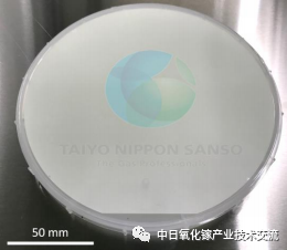
Fig. 1 Film forming on 6-inch test wafer β-Ga2O3 film
NCT, TAIYO NIPPON SANSO and Tokyo University of Agricultural and Technological developed a 6-inch blade type HVPE device (Figure 2), which was successfully achieved β-Ga2O3 film formation on a 6-inch test wafer (using sapphire substrate) for the first time in the world (Fig. 1).
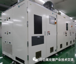
Figure 2: Appearance photo of 6-inch monolithic HVPE device for β-Ga2O3 film forming
In addition, by optimizing film forming conditions and the use of an independent raw material nozzle structure, it was confirmed that β- Ga2O3 film formation can be achieved, and confirmed that β-Ga2O3 film thickness distribution can be controlled in the range of less than ± 10% in the plane. The film forming technology and hardware design technology on large-diameter substrate established by this achievement can build the platform of β-Ga2O3 film forming device, so the development of large diameter batch production device can make great progress. So, with the reduced power consumption brought by β-Ga2O3 film forming process and application equipment, it is estimated that the energy saving will reach about 210000 kL/year in 2030.
