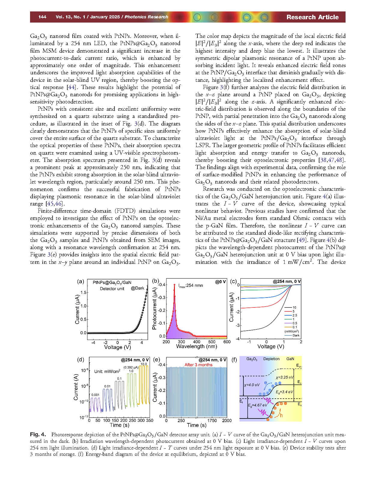
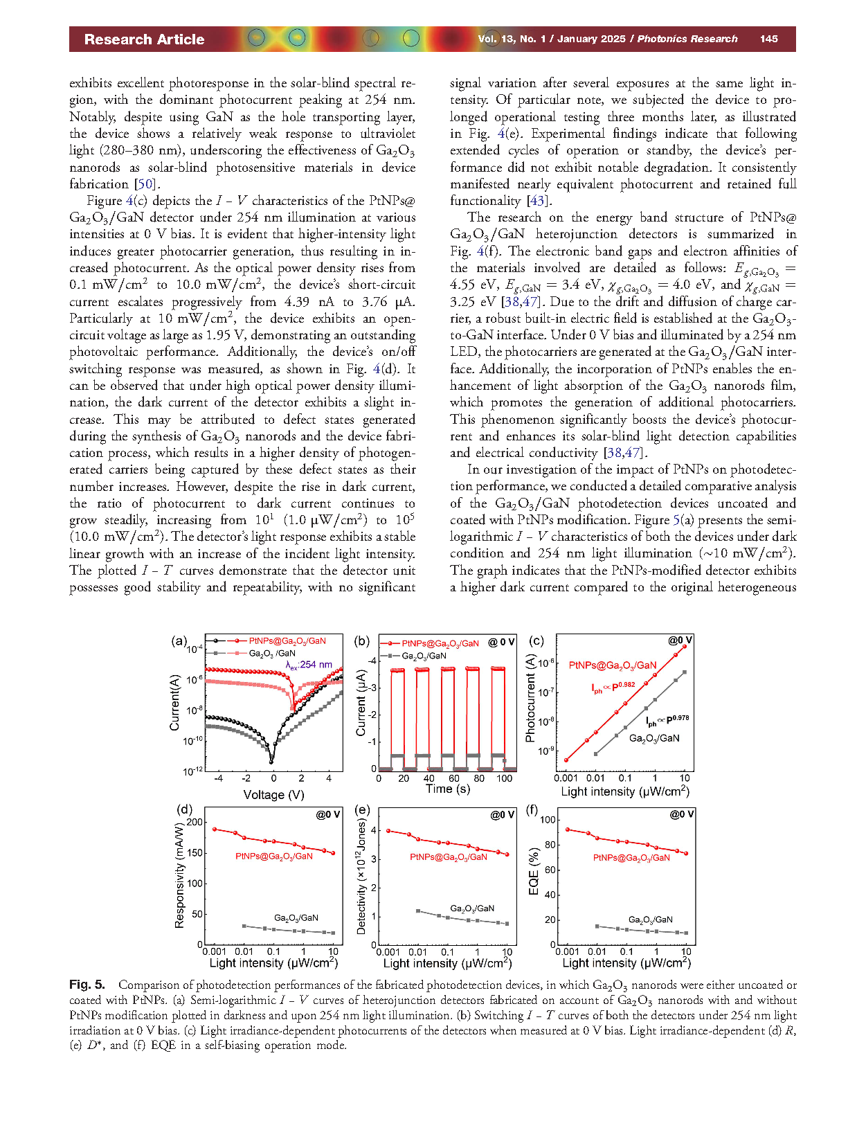
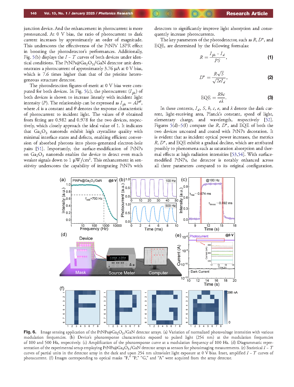
Paper Sharing
【Domestic Papers】 Nanjing University——Plasmonically enhanced solar-blind self-powered photodetector array utilizing Pt nanoparticles-modified Ga₂O₃ nanorod heterojunction
日期:2025-02-18阅读:870
Researchers from the Nanjing University of Aeronautics and Astronautics have published a dissertation titled "Plasmonically enhanced solar-blind self-powered photodetector array utilizing Pt nanoparticles-modified Ga2O3 nanorod heterojunction" in Photonics Research.
Abstract
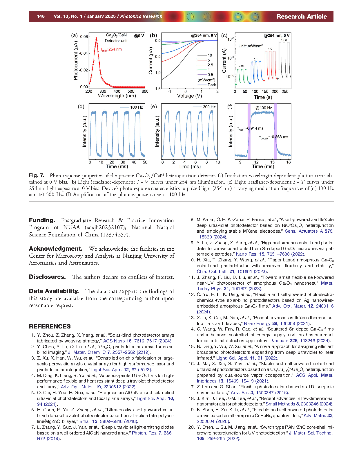
Low-dimensional Ga2O3 monocrystalline micro/nanostructures show promising application prospects in large-area arrays, integrated circuits, and flexible optoelectronic devices, owing to their exceptional optoelectronic performance and scalability for mass production. Herein, we developed an 8×8 array of high-performance solar-blind ultraviolet photodetectors based on Pt nanoparticles-modified Ga2O3 (PtNPs@Ga2O3) nanorod film heterojunction with p-GaN substrate serving as the hole transporting layer. The PtNPs@Ga2O3/GaN heterojunction detector units exhibit outstanding photovoltaic performance at 0 V bias, demonstrating high responsivity (189.0 mA/W), specific detectivity (4.0×10¹² Jones), external quantum efficiency (92.4%), and swift response time (674/692 µs) under an irradiance of 1 μW/cm2 at 254 nm. Their exceptional performance stands out among competitors of the same type. In addition, the detector array demonstrated satisfactory results in a conceptual demonstration of high-resolution imaging, benefiting from the excellent stability and uniformity exhibited by its array units. These findings provide a straightforward and viable method for developing a high-performance solar-blind ultraviolet detector array based on low-dimensional Ga2O3 nanorod monocrystalline, demonstrating their potential advancement in large-area, integrable, and flexible optoelectronic devices.
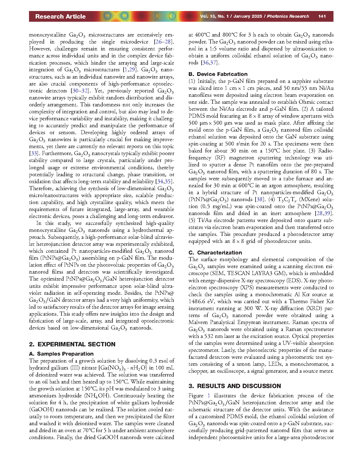
Fig. 1. Schematic illustration of the preparation process for the PtNPs@Ga2O3/GaN detector array and the structural diagram of the detector unit.
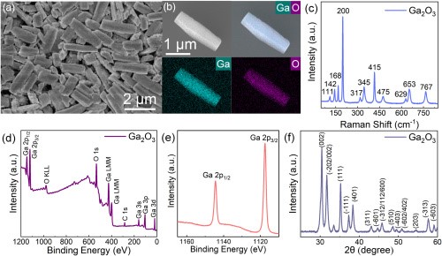
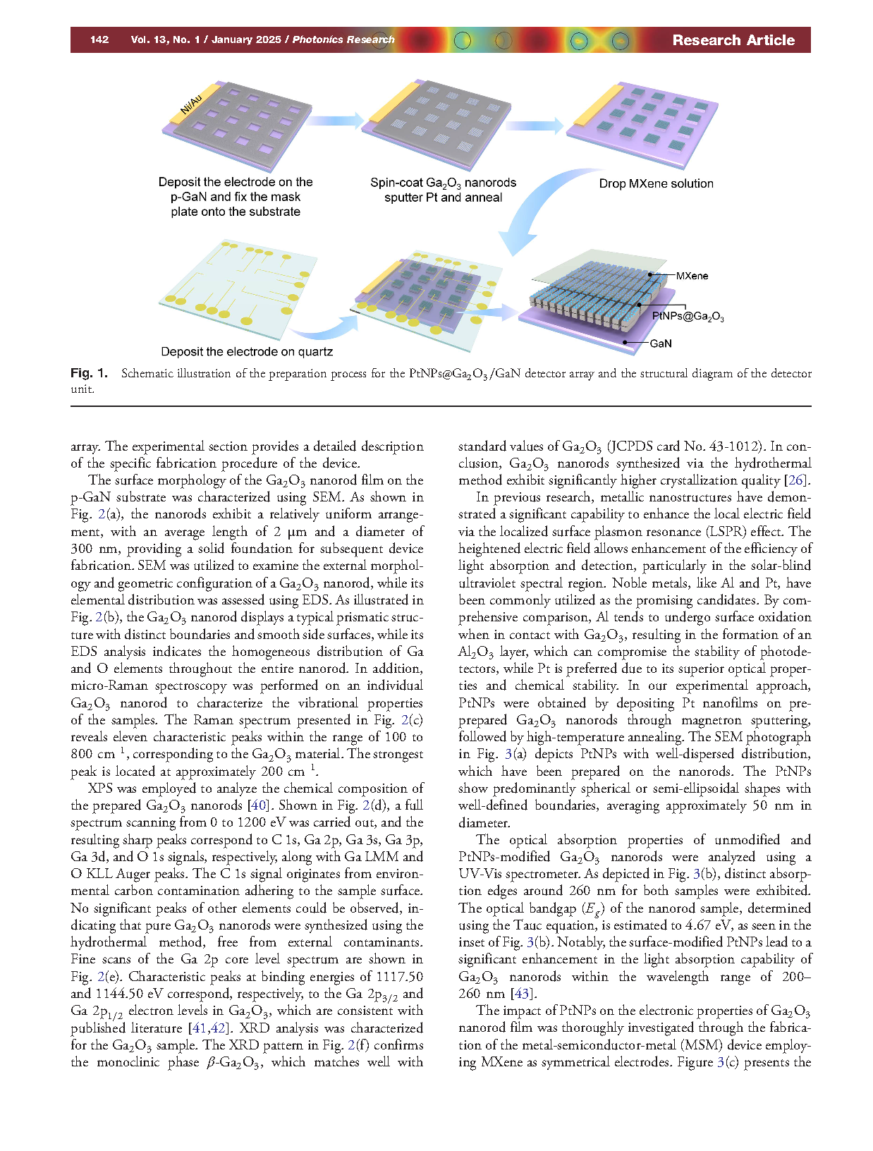
Fig. 2. Ga2O3 nanorod characterization. (a) SEM image of Ga2O3 nanorods film. (b) SEM image and EDS mapping of a Ga2O3 nanorod. (c) Raman spectrum of Ga2O3 samples. (d) Comprehensive XPS spectrum of the Ga2O3 nanorods. (e) XPS analysis focusing on Ga 2p lines of Ga2O3 nanorods. (f) XRD pattern of Ga2O3 nanorods.
DOI:
doi.org/10.1364/PRJ.539310