


Member News
【Member News】New Breakthrough in iSABers Bonding Technology: Hybrid Bonding and C2W Technology Lead Industrial Upgrading
日期:2025-02-19阅读:1343
In recent years, the semiconductor industry with its rapid development momentum, has become the focus of the field of science and technology. With the rise of emerging technologies such as 5G, Internet of Things and artificial intelligence, the requirements for chip performance are increasing day by day, and advanced bonding technology, as a key link to improve chip performance and reduce costs, is increasingly receiving extensive attention from the industry. Recently, the semiconductor industry has made significant progress in the field of advanced bonding technology, especially the breakthrough of hybrid bonding and C2W (Chip-to-Wafer) technology, which has injected new vitality into industrial upgrading.
Hybrid Bonding Technology: A New Milestone in Semiconductor Interconnection
Hybrid bonding technology, as an innovation in the field of advanced bonding, its basic principle is to achieve efficient interconnection between chips by bonding chips of different materials or different processes with high precision and high reliability. This technology not only improves the integration of the chip, but also significantly enhances the thermal and electrical properties of the chip. In emerging fields such as artificial intelligence and the Internet of Things, hybrid bonding technology, with its unique advantages, is gradually becoming a key technology to improve device performance and reduce power consumption.
As a pioneer in this field, iSABers has reached an industry-leading level in its hybrid bonding technology. The company has successfully conquered key technologies such as high precision and fast alignment, precise control of bonding offset, intelligent compensation of wafer deformation, and high efficiency surface activation. These technological breakthroughs not only improve the performance of products, but also provide customers with more reliable and efficient chip solutions.
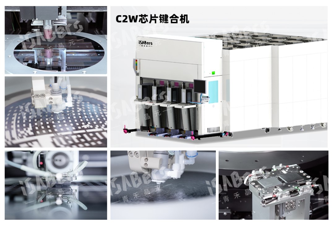
C2W Technology: Simplify Processes and Improve Efficiency
C2W (chip to wafer) bonding offers more flexibility than W2W (wafer to wafer), allowing for individual testing and screening of high-quality chip rebonding, reducing the overall defect rate. Support heterogeneous integration (different process node/size chip combination), reduce material waste, reduce costs, improve efficiency.
Its self-developed 12-inch C2W wafer bonding machine has an alignment accuracy of ±50nm, and the bonding accuracy is better than 100nm after bonding. The innovative bottom-up bonding method can avoid bonding surface contamination during the chip flipping process and reduce particle increase value. Compared with the traditional C2W bonding technology, the new technology improves the bonding yield, further proving the company's strength in the field of advanced bonding technology.
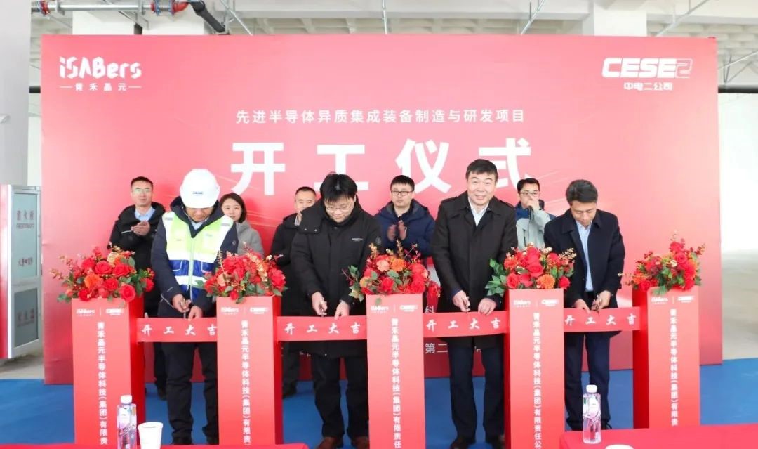
iSABers New Plant Started, Support Industrial Upgrading
Recently, the opening ceremony of the new plant of iSABers was just held. According to official reports, the project started this time is the bonding equipment phase II expansion line and headquarters office construction project, with a planned total area of 17,000 square meters. After the project is completed and put into operation, it is expected to produce about 100 sets of advanced semiconductor equipment annually, with an annual output value of nearly 1.5 billion yuan.
The completion of the new plant will greatly expand the production capacity of iSABers and enhance the research and development capacity. The new plant can meet the continuous production of multiple types of equipment such as W2W hybrid bonding, C2W hybrid bonding and high-precision flip chip bonding, ultra-high vacuum normal temperature wafer bonding, hot pressing anode wafer bonding, etc., to meet the market demand for high-end bonding equipment. At the same time, the new plant will also introduce an intelligent management system to further improve production efficiency and product quality.
Semiconductor Bonding Technology Outlook: Innovation Leads the Future
Looking ahead, semiconductor bonding technology will continue its rapid development momentum. New technologies such as hybrid bonding and C2W will continue to push the industry forward and provide more diversified and higher performance chip solutions for smart home, automotive electronics, medical electronics and other fields.
With continuous breakthroughs and innovations in the field of advanced bonding technology by companies such as iSABers, the semiconductor industry is expected to achieve leapfrog development in the next few years. We will see more high-performance, low-cost chip products emerge, providing strong support for the development of various industries. At the same time, new technologies will also promote the coordinated development of upstream and downstream companies in the semiconductor industry chain, forming a more complete industrial ecology.
We encourage readers to follow the latest developments in the semiconductor industry and witness the brilliant future of the industry together. It is believed that in the near future, the semiconductor industry will usher in more innovation and development opportunities, and make greater contributions to the progress of human society.
