Discover
【Knowledge Discover】Core Technology Affecting Semiconductor——Observation of Crystal from the Perspective of Symmetry (1)
日期:2025-02-24阅读:3899
Reading Guidance
Knowledge Discover is a new popular science column launched by the official account, focusing on in-depth analysis of cutting-edge materials and basic science. We will focus on the emerging semiconductor material of "Gallium Oxide", from crystal structure, physical properties to application scenarios, to comprehensively understand its breakthrough potential in fields such as 5G communication and new energy vehicles. At the same time, the column will also explore the scientific principles of Gallium Oxide materials and reveal their wide applications in energy, environmental protection, electronics and other fields.
Profile of Original Author
Hajime Okumura,Doctor of Engineering (Osaka University). Representative of Innovative Semiconductors, Electronics, & Energy Solutions, a limited liability partnership. Honorary Researcher of National Institute of Advanced Industrial Science and Technology. Honorary Associate Professor of University of Tsukuba.
1.Introduction
In recent years, the importance of semiconductor technology has been put forward again, and the semiconductor crystal preparation technology as the basic material is an indispensable core technology. People usually directly associate the "semiconductor" with the semiconductor chip, but in ensuring the performance of the semiconductor chip, it is particularly important to improve the quality of the semiconductor crystal as the basic material. Whether it is an optical device or an electronic device, its performance is based on the characteristics of the semiconductor material "crystal". By making full use of the characteristics of the crystal, the maximum performance of the semiconductor chip can be brought into play. At the atomic level, a "crystal" is a solid that has a specific unit structure (called a " unit cell ") and is arranged regularly in space (in other words, has translational symmetry). In the case of semiconductor crystals, their properties are largely affected by the regularity of the crystals themselves. Because semiconductor crystals need to enhance their integrity by eliminating various crystal defect that impair the regularity. Therefore, it is no exaggeration to say that the semiconductor crystal manufacturing technology that can achieve perfect crystallization is the core technology as an advanced semiconductor.
In the preparation of large crystals of various sizes for actual use, the ideal state is that the whole region of the crystal remains perfect (that is, the translation symmetry of the cell is throughout the crystal). However, in the actual crystal growth process, the polymerization of tiny grains usually occurs. In this case, the realization of the "regular arrangement" of crystals is the ultimate goal pursued by semiconductor crystal engineering. However, in the grain boundary region, it is often that crystal defects occur due to the difficulty in maintaining translational symmetry (that is, it is impossible to overlap the adjacent hexahedron under parallel movement of the hexahedron). Or the interruption of translation may occur during the process of crystal growth due to the occurrence of crystal defects. As crystal growth progresses, defect propagate gradually and even extend to the surface, ultimately affecting the performance of the semiconductor chip, especially in terms of initial performance and long-term reliability.
Looking back at the development of semiconductor technology from the perspective of semiconductor crystals, initially with germanium (Ge), followed by silicon (Si) technology has made great progress. Today, near-perfect crystals have been achieved on the silicon side, and these high-quality large-size silicon crystals are widely used in large-scale integrated circuits (LSI) in the current mainstream semiconductor technology. However, due to the limitations of silicon materials in terms of performance improvement, especially in optical devices and high-frequency applications, III-V compound semiconductors represented by Gallium Arsenide (GaAs) have been studied, and these materials have gradually been applied. Subsequently, with the increase in demand for short-wavelength optical devices and power applications, wide bandgap semiconductors such as Gallium Nitride (GaN) and Silicon Carbide (SiC) began to receive attention, and gradually developed semiconductor devices based on these materials. At present, in the field of power applications, the development of Gallium Oxide (Ga2O3), Aluminum Nitride (AlN) and Diamond semiconductors is also steadily advancing, broadening the field of power applications.
Re-examining the development process of the above semiconductor materials from the perspective of crystal structure, it is not difficult to find some interesting characteristics. The earliest Ge and Si were elemental semiconductors, crystals with Diamond structures. The III-V compound semiconductors that emerged later, such as GaAs, are binary compounds, but their structure is similar to the sphalerite structure of Si, and these materials have a higher symmetric cubic crystal system structure. The GaN and SiC after that are mainly wurtzite crystals with hexagonal structure. The Ga2O3, which appeared later, showed a corundum structure of the triangular crystal system, or a monoclinic crystal system, which was significantly different from the previous materials.

Table 1-1 Crystal structures of various semiconductor materials
The crystal structures of these semiconductor materials are shown in Table 1-1 (details will be discussed later) and range from relatively simple structures to quite complex structures. To illustrate here, as a rough metaphor, imagine the process of put multiple parallelepipedrons (hereinafter referred to as "hexahedrons") with cell shapes specific to the crystal system into a box (see Figure 1-1). It is difficult to get many hexahedrons to line up neatly if they are put into a box in a disorganized manner. However, if external stimuli are given by shaking the box, etc., a certain degree of regular alignment can be achieved, although not necessarily completely neat. And, if the hexahedron is shaped like a cube like a dice, it will be easier to arrange (and, conversely, harder if the hexahedron is irregularly shaped).
In addition, a case can be considered, as shown in Figure 1-2, in which one of the hexahedrons (crystals) in a regular arrangement can be assumed to be removed, rotated to change its attitude and then replaced. If it is a cube, even if it is rotated 90° around a specific axis, its vertices will exchange with each other, but the relative position of the overall spatial axes (x, y, z axes in the figure) will not change, so it can be directly integrated back into the crystal in its original attitude. However, for ordinary hexahedrons, even if the same rotation operation is performed, they cannot be directly reintegrated into the crystal.
It can be inferred that if hexahedrons have high symmetries like cubes (figuratively understood as "eight vertices make no difference"), they will be more easily arranged into regular structures. This kind of intuitive thinking might help us understand the regularity of crystal arrangements.
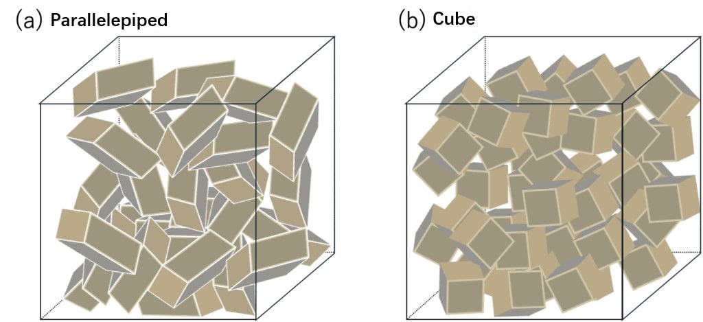
Figure 1-1 Schematic diagram of loading parallelepiped into a box.
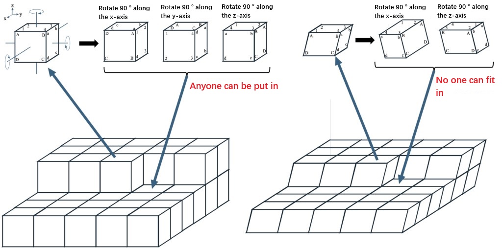
Figure 1-2 The process of placing a parallelepiped in a regular three-dimensional arrangement. If it is a cube, its orientation will not change after a rotation operation, and it can be arranged regularly, but a general parallelepiped cannot have its orientation arranged regularly after a similar rotation operation.
Figure 1-3 shows the partially symmetrical elements of a hexahedron and a cube. For example, in terms of rotational symmetry, a cube has a quadruple or triple axis of symmetry, while a hexahedron has only a center of inversion. In other words, it is easier for cubes to maintain the same posture than hexahedrons, making regular arrangements easier to achieve. That is, when crystals have higher cell symmetry, they are better able to fill the three-dimensional space while maintaining translational symmetry, which means that complete crystals without defect (i.e. perfect crystals without defect) can be formed. The crystal structure of each material is characterized by a combination of symmetric elements: a "Bravais lattice" to express the symmetry of the cells, a point group representing the symmetry of the "Motif" on the lattice points, and a "space group" formed by a combination of Bravais lattice and point groups. First, we can consider whether the cell symmetries expressed by the lattice fit to fill the space (i.e., the translational group problem). Second, we can also consider how the symmetry of the basic structure and the directionality of the chemical bonds (i.e., the point group problem) affect the arrangement of cells. The number of symmetric elements that a space group possesses may be an indicator of how good or bad the symmetry is. Through a large number of illustrations, this paper will focus on the commonalities and differences among these semiconductor materials, from the perspective of crystal symmetry (that is, whether the crystals can fully coincide under translation or rotation operation) and the occurrence of crystal defect accompanying the epitaxial growth process, and integrate some unique perspectives. In other words, this is a kind of discussion in the three-dimensional space like building blocks, I hope readers can easily read on. In Part (2), we will discuss cubic crystals; Part (3) will cover hexagonal crystals; Other types of crystals will be discussed in part (4), and finally concluding with a summary.
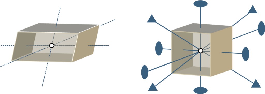
Figure 1-3 Illustrates symmetries of hexahedrons and cubes in general.
· Represents the double axis of rotation, ▲ represents the triple axis of rotation, and ○ represents the center of reversal.
The explanation of crystallography specific terms and basic concepts is too tedious to be detailed in this article, but is listed in the Appendix at the end of the article (Appendix 1, 2, 3), please refer to the Appendix for details. In addition, please understand that this discussion is limited to morphologic crystallography, although it may be necessary to consider energetics in order to fully understand phenomena.
2.Crystal Growth and Crystal Symmetry
Next, how is symmetry maintained during actual crystal growth? Let's revisit the meaning of crystal growth. In order for the tiny groups of atoms from which crystals are made to grow into macroscopic solid crystals, these "dot" -like atoms groups need to somehow come together in the first place. Natural nuclear formation initially occurs in what is called "Seedless Crystal Growth", which can be understood as groups of atoms coming together in free space in no particular direction. However, unless it is an amorphous structure, even naturally occurring nuclei should retain the symmetry of crystals on a microscopic scale. Once a naturally occurring nucleus with crystalline properties reaches a certain size, subsequent growth can be understood as growth along a crystal face (with little possibility of growth at the apex or edge). Therefore, the following discussion will assume the crystal as substrate in the case of " Seedless Crystal Growth" and will discuss the growth of the crystal on a specific crystal face on the surface of the substrate crystal.
In crystal growth on a two-dimensional surface, the phenomenon of film growth in which information about the crystal structure of the lower substrate is transmitted to the upper growth layer is called Epitaxial Growth. At the microscopic level, epitaxial growth is known in three main ways:
(1) Island Growth (Volmer-Weber type)
(2) Layered Growth (Frank-von der Merwe type)
(3) Compound Growth (Stranski-Krastanov type)
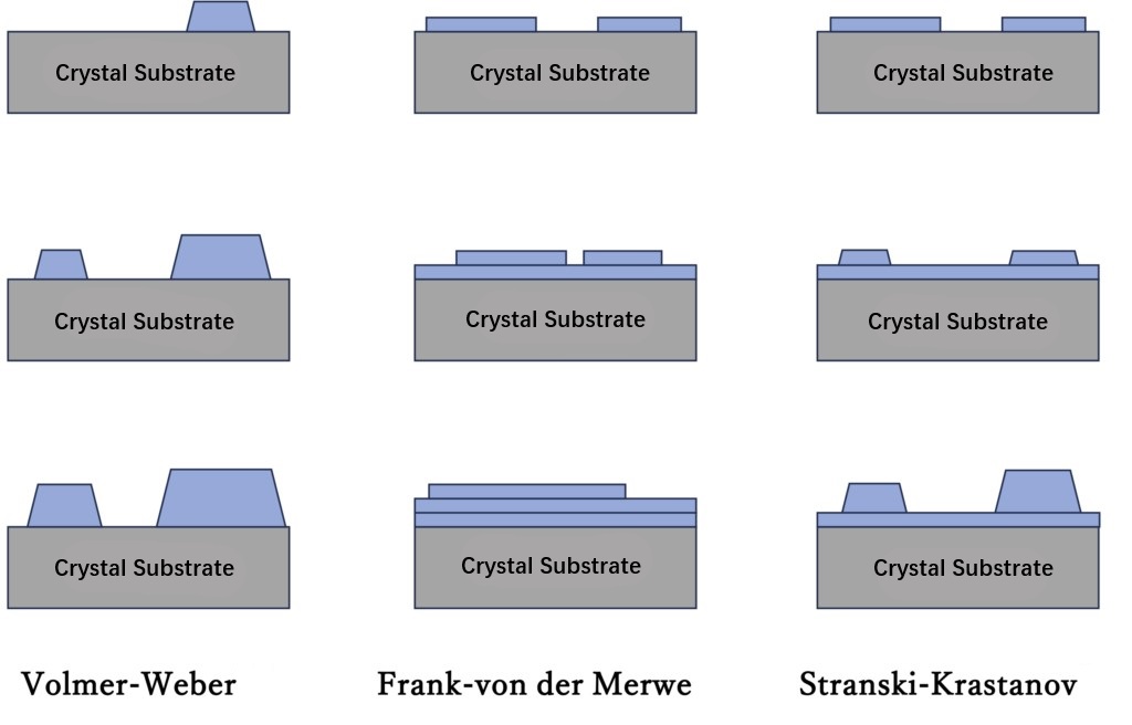
Figure 1-4 Growth pattern of epitaxial growth. The first row shows total growth of less than 1 atomic layer, the second row shows 1-2 atomic layers, and the third row shows more than 2 atomic layers.
These situations are illustrated in Figures 1-4. In order to achieve the ideal epitaxial growth, (2) layer growth is necessary, and then layer upon layer to form a complete crystal. However, it is extremely difficult to fully achieve the layered growth of (2) at macro-scales up to the wafer level. Even if a perfectly flat crystal substrate surface as shown in Figure 1-4 can be prepared, "Domain A" may form in one area on the substrate and a different "Domain B" may form in another. Although layered growth may be achieved within the region, island-like regions may still form on a macro scale. This is because even the initial crystal substrate cannot be completely flat at the atomic level, often resulting in atomic-level steps. The two growth domains are basically the same in material and structure as the epitaxial growth layer on the underlying substrate. As the growth progresses, the two domains will collide at some point. Figure 1-5 illustrates this situation. Since the starting point of the island region is different in Domain A and B, there will be no direct propagation relationship between domains A and B, such as the epitaxial structure, during this process. Ideally, if the structural information of the substrate can be accurately transmitted to Domains A and B, then even if A and B collide, the translational symmetry of the crystals between them can still be maintained, thus forming a complete single crystal. However, if there is some kind of crystal growth "error" in one of the regions during the layered growth process, it is not guaranteed that Domain A and B have the same symmetry, which may cause the translation symmetry of the crystals at the merging boundary to be broken. In addition, factors such as the strain of the substrate may cause the crystal axes of the two domains to shift slightly. In this case, the merging boundary becomes a defect of the crystal.
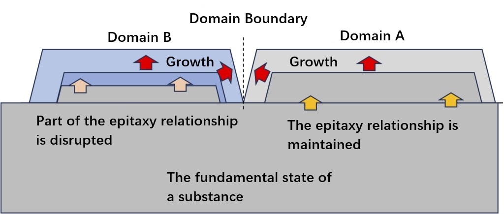
Figure 1-5 Collision of different growth regions in the actual epitaxial growth process.
In epitaxial layered growth, the structural information conveyed by the stacked layers is basically derived from the surface layer of the underlying substrate. By passing structural information about this layer (including symmetry), layer by layer during the stacking process, three-dimensional crystals are formed. In simple terms, the symmetry of the layers here is equivalent to the symmetry of "wallpaper that can be completely overlaps by translation", which is systematically summarized in the two-dimensional plane group (to be precise, it is the "layer group" with both sides, see Int. Tables for Crystallography, Volume E). This "layer group" information can be understood as being transformed into a three-dimensional "space group" when stacked layer by layer. However, since the layer group itself does not contain the information of stacking direction, it will not completely match the space group of the original crystal structure in the stacking process. This mismatch is the essential reason for the "error" in the crystal growth process mentioned above. Like the three-dimensional crystal structure, the two-dimensional layer structure can also be represented by "lattice + motif". Therefore, in the following discussion, we will show the two-dimensional net (lattice) in the frequently used two-dimensional plane in Figure 1-6. They correspond to Bravais lattices in three-dimensional space, and are divided into five types, as shown in Figure 1-6.
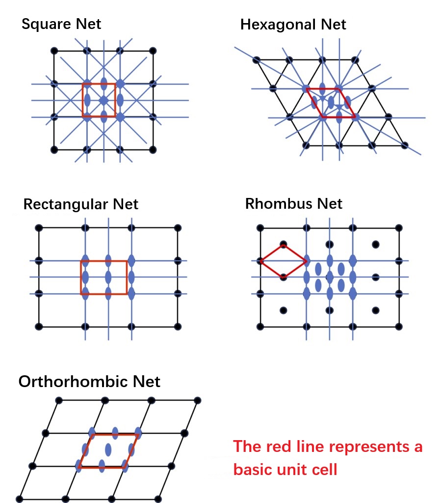
Figures 1-6 Represent the various two-dimensional nets of two-dimensional planar lattice structures and their symmetric elements.
As the first part of a series of articles, this paper presents the problems and investigations in the epitaxial growth of semiconductor materials from the perspective of crystal symmetry. The following contents will be combined with actual semiconductor crystal growth examples, one by one to introduce the crystal structure characteristics, commonness and differences of various semiconductor materials, and will also compare and analyze the influence of crystal structure and growth layer symmetry on epitaxy growth.
References
- “物質の対称性と群論”: 今野豊彦(Kyoritsu Publishing, 2001)
- “Int. Tables for Crystallography, Volume A, 6th edition”: Eds. M.I. Aroyo (Wiley, 2016)、 On-line: https://it.iucr.org/services/purchase/
- “Int. Tables for Crystallography, Volume E, 2nd edition”: Eds. V. Kopsky and D.B. Litvin (Wiley, Dec. 2010)
Appendix 1
The following information is essential when discussing crystal symmetry.
· Lattice
In a crystal, locations with the same surrounding environment can be represented by points, which are called lattice points, and the collection of lattice points is the lattice. There is a certain arbitrariness to the selection of lattice points, and atoms do not necessarily always appear on the lattice points. In addition, the entire lattice can be represented as a collection of suitable parallelepipeds composed of the lattice points, called a Unit Cell. There is also a degree of arbitrariness in the choice of cells, but usually the cell with the symmetry that as high as possible is chosen. The smallest of all cells that contains a lattice point (where the lattice point on an edge or vertex is split into multiple cells) is called a basic cell. To represent a parallelepiped, the three sides connected by a vertex can be defined as vectors, starting from that vertex as the A-axis, B-axis, and C-axis, respectively (the standard is right-handed). The length of the vector (translation vector) corresponding to the A-axis, B-axis and C-axis is called a, b, c, and the Angle between them is called α, β, γ, respectively, and these parameters are collectively called the lattice constant. The vectors between any lattice points are called translation vectors, and integer multiples of translation vectors are also considered translation vectors. The vectors representing the three sides of the basic cell are called the basic translation vectors.
· Motif
In a crystal, a collection of atoms, etc. (including atoms, ions, or molecules) arranged at lattice points is called a motif. When discussing symmetries, it is important to properly define the range of the motif and their positions with respect to the lattice points. The motif can be described by the symmetries around one of these points.
· Crystal Structure
Crystal structure is a description of the arrangement of atoms, etc., inside a crystal. The crystal structure can be represented by defining the lattice and the motif (the set of atoms, etc.) that are configured at all lattice points. To wit:
Crystal Structure = lattice + Motif
In a crystal, the translation symmetry defined by the basic translation vector and the symmetry around the lattice points are preserved, and the crystal structure is characterized by this symmetry.
· Lattice Structure
A lattice structure is determined by the arrangement of the lattice points that make it up. The most basic is the simple lattice, the parallelepiped. To maintain translational symmetry, simple lattices can be combined with other simple lattices by moving in parallel (called centralization), and this moved lattices are called sublattices. For more intuitive expression, simple lattices are often combined into composite lattices for ease of understanding. There are four types of composite lattices: body-centered lattice, face-centered lattice, base-centered (side-centered) lattice, and orthorhombic lattice. If the unit cell is a composite lattice, though with reduced symmetry, it can be broken down into smaller elementary unit cells. In a composite lattice, it is common to treat the composite lattice itself as the unit cell, rather than the fundamental unit cell, and determine the lattice constant by defining its three vectors. The number of sublattices in each composite lattice and their amount of movement will be shown below.
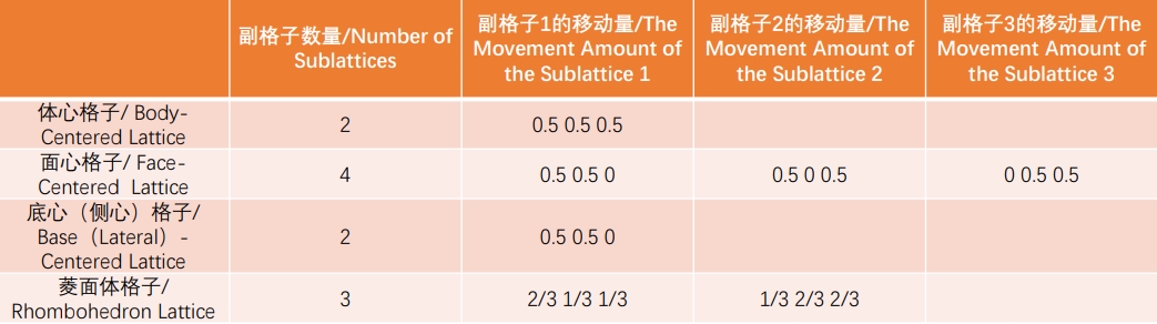
The above movement amounts are conceptual values obtained by considering the lengths of each crystal axis as 1
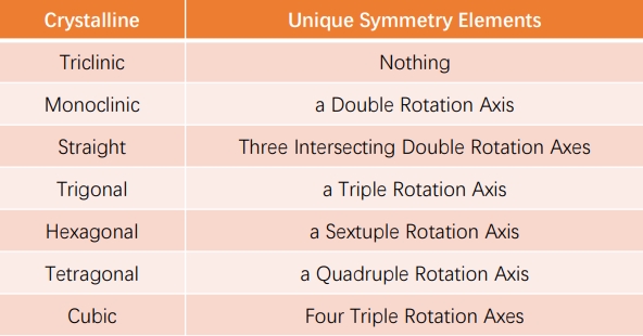
· Symmetries of Lattices and Crystal Systems, Bravais Lattices
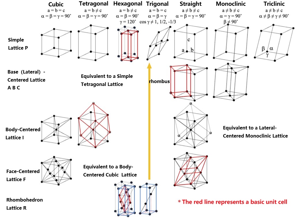
Based on the symmetry of the lattice (the relationship of a, b, c, α, β, γ), the lattice can be classified into seven crystal systems: triclinic, monoclinic, straight (rhombic), tetragonal, hexagonal, trigonal, and cubic (equiaxial), each with its own characteristic symmetry operation of crystalline point groups. Through the combination of lattice types and crystal systems, in addition to the equivalent case, fourteen kinds of lattice called Bravais lattice are derived (as shown in the following figure). As illustrated by the hexagonal columns in the simple lattice of hexagonal crystals, this is not a composite lattice or (basic) unit cell. The rhombohedral body lattice can be represented as a composite lattice of the simple hexagonal lattice, but it is usually represented as a trigonal system of an easily understood quadrilateral prism (indicated by the red line) that is inconsistent with the basic unit cell. For a simple trigonal lattice, γ becomes one of the other Bravais lattice with higher symmetry when it has a special value. For example, cos γ = 0 (γ = 90˚) is a simple cubic lattice, 1/2 (γ = 60˚) is a face-centered cubic lattice, and -1/3 (γ = 109.47˚) is a body-centered cubic lattice. In monoclinic systems, γ ≠ 90˚ is sometimes accepted as a convention, and in some cases, β ≠ 90˚ can be chosen. In the figure below, β ≠ 90˚ is the default choice, showing the symmetry elements that are unique to each crystal system.