


Member News
【Member News】Mass Production of A New Generation of Power Semiconductor Material 'Gallium Oxide' 4-inch Wafer
日期:2023-03-06阅读:1119
NCT produces 20000 pieces a year.
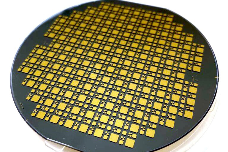
4-inch Ga2O3 epitaxial wafer
NCT (Sayama, Saitama, President: Akito Kuramata) plans to mass produce 20000 pieces of 100 mm (4 inches) gallium oxide (Ga2O3) epitaxial wafers per year till 2025. Our factory will add additional equipment with the investment amount about 2 billion yen. As a new generation of power semiconductor, gallium oxide is expected to become a material that can reduce the cost. It will also promote technological development aimed at mass production of 6-inch wafers.
In addition to the equipment and testing equipment for manufacturing and processing Ga2O3 single crystal substrates, the epitaxial equipment for epitaxial growth of Ga2O3 on wafers will also be introduced. It is planned to develop new equipment capable of producing multiple epitaxy at the same time in 2022, and these equipment will be gradually introduced in the general plant.
Compared with traditional silicon semiconductor, gallium oxide semiconductor can achieve lower device power consumption and higher breakdown voltage. Single crystal can be grown by melting method, and single crystal wafer can be manufactured effectively. Compared with the next generation materials such as silicon carbide (SiC) currently in use, the crystal growth rate is about 100 times faster, and the substrate is easier to manufacture, resulting in a significant reduction in cost.
NCT is a subsidiary of Tamura. For the first time in the world, the company successfully produced 4-inch Ga2O3 wafers. It includes Schottky barrier diodes (SBDs) capable of withstanding up to 1200 volts developed in 2021, and participating in the research and development of power devices. The company also plans to commercialize high-voltage diodes in 2023 and transistors in 2025.
