Member News
【Member News】Zhang Hezhi, a Teacher of Dalian University of Technology, Made New Discovery on the Growth of Gallium Oxide
日期:2023-03-16阅读:1210
Profile
Associate Professor Zhang Hezhi graduated from the Université Paris XI, France, with a doctor's degree in 2016, and studied from researcher Maria Tchernycheva. In the same year, he joined the research group of Professor Nicolas Grandjean of the University of Technology in Lausanne, Switzerland, to engage in post-doctoral research. In October 2019, he joined the research team of wide band-gap semiconductors, Professor Liang Hongwei, School of Microelectronics, Dalian University of Technology. At present, he is mainly engaged in the research on the growth of ultra-wide band gap semiconductor Ga2O3 materials and devices.
Introduction
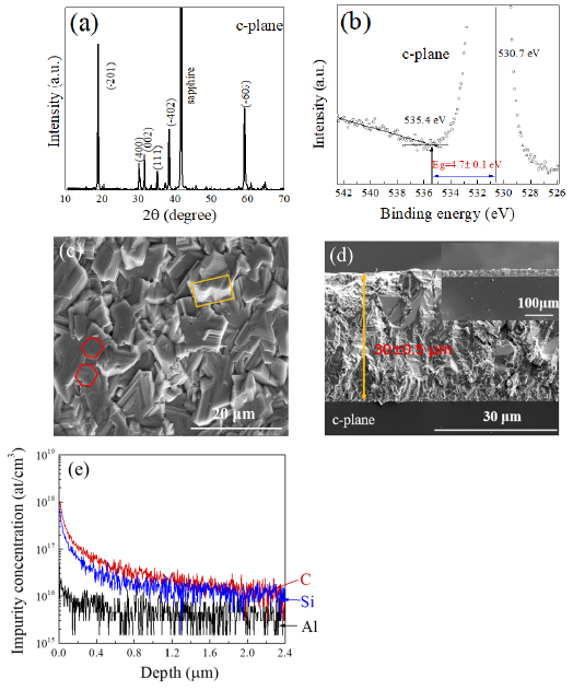
Gallium oxide (Ga2O3) as an ultra-wide band gap semiconductor has important application prospects in high-voltage power devices, Solar-blind ultraviolet communication and radiation detection. At present, growth β- Ga2O3 thick film is mainly grown by halogenated vapor phase epitaxy (HVPE), in addition to this method, the report of growing β-Ga2O3 thick film by other methods is still rare. In this paper, we use carbon reduction vapor phase method to grow β-Ga2O3 thick film. The basic principle of it is that Ga2O3 powder is reduced and decomposed into gallium (Ga) vapor and oxygen (O2) at high temperature, and Ga2O3 is grown by the reaction of Ga vapor and O2 at low temperature. In the experiment, the high temperature zone is set at 1450 ℃, the low temperature zone is set at 900 ℃, and the growth time is 2 hours. The results of X-ray diffraction (XRD) are shown in Fig. 1 (a). The growth of β- Ga2O3 films on C-plane sapphire substrate by sublimation method have preferred orientation along (- 201). Deduced by the energy loss spectrum of O1s core energy level in X-ray energy spectrum (XPS) , the band gap width of β-Ga2O3 film is about 5 eV (as shown in Figure 1 (b)). The surface morphology and thickness of β-Ga2O3 sublimated were characterized by scanning electron microscopy (SEM). Surface SEM shows the β-Ga2O3 film has a quasi-hexagonal lattice structure with obvious grain boundaries, as shown in Fig. 1 (c). The film thickness of about 27μm can be observed through section SEM (Fig. 1 (d)). The growth rate is about 14 μm/h。According to SIMS test (Fig. 1 (e)), although the process of carbon reduction was introduced into the growth, in addition to certain carbon enrichment on the surface of the grown thick film, the carbon residue in the thick film has reached the limit of SIMS test , which can be almost ignored. The results above show that the carbon reduction vapor phase method has the potential to grow Ga2O3 thick films.