Member News
【Member News】Global Debut | Releases First 8-Inch Gallium Oxide Single Crystal, Ushering in a New Era of Gallium Oxide
日期:2025-03-06阅读:3106
On March 5, 2025, Hangzhou GAREN SEMI Co., LTD. (hereinafter referred to as "GAREN SEMI") released the world's first fourth-generation semiconductor Gallium Oxide 8-inch single crystal. GAREN SEMI has successfully achieved the growth of 8-inch Gallium Oxide single crystal using a completely independent and innovative casting method, and can process the corresponding size of the wafer substrate. This achievement marks that GAREN SEMI has become the first enterprise in the world to master 8-inch Gallium Oxide growth technology, refreshing the global record for Gallium Oxide size, and creating an industry record for upgrading one size every year from 2 inches to 8 inches.
China's Gallium Oxide took the lead in entering the 8-inch era, which has far-reaching industrial significance.
First, the 8-inch Gallium Oxide can be compatible with the 8-inch production line of existing silicon-based chip plants, which will significantly accelerate the pace of its industrial application.
Secondly, the increase of Gallium Oxide substrate size can improve its utilization rate, reduce production costs, and improve production efficiency.
Finally, China took the lead in breaking through the 8-inch technical barrier, which not only marks China's technological progress in the field of ultra-wide band gap semiconductors, but also our Gallium Oxide industry has seized the lead in the global semiconductor competition, and effectively promoted China's dominant position in the global semiconductor competition pattern.
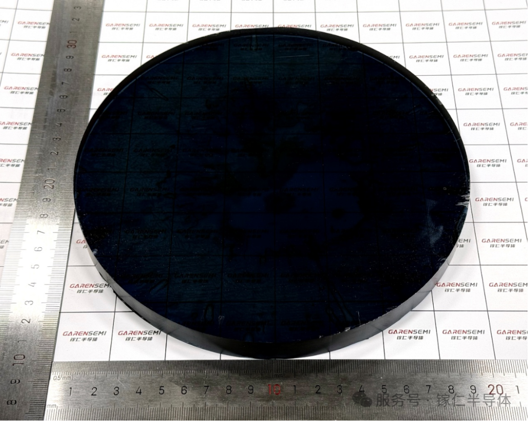
Figure 1 GAREN SEMI 8-inch Gallium Oxide single crystal
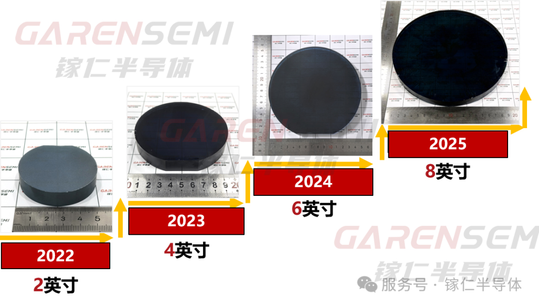
FIG. 2 Rapid evolution of GAREN SEMI Gallium Oxide single crystal size
Ⅰ Introduction to Gallium Oxide
Semiconductor material is the basis of modern information technology and the development of electronic information industry, is an important sign to measure a country's scientific and technological level and comprehensive national strength. Has experienced the development of semiconductor materials represented by Si, Ge, the first generation of semiconductor materials, the second generation of the compounds represented by GaAs, InP, as well as represented by SiC, GaN of the third generation of wide bandgap semiconductor materials. In recent years, as new energy, photovoltaic power generation, radar detection, 5G with the rapid development of mobile communications and other fields, represented by gallium oxide (β-Ga2O3) has forbidden band width and higher breakdown electric field intensity of ultra wide band gap semiconductor materials, began to attract wide attention from all walks of life and value.
01 Gallium Oxide (β-Ga2O3) Has Excellent Physical Properties
The band gap of Gallium Oxide single crystal is about 4.8eV, and the breakdown electric field strength is about 8MV/cm, which is much higher than Si(1.1eV, 0.3MV/cm), SiC(3.3eV, 2.5MV/cm), GaN(3.4eV, 3.3MV/cm) and other materials. The power device produced has higher working voltage and power.
Moreover, the BFOM of Gallium Oxide is about 10 times that of SiC and 4 times that of GaN. The devices developed using Gallium Oxide will have smaller on-resistance and higher power conversion efficiency.
The UV cut-off edge of Gallium Oxide single crystal is short (260nm), and the transmittance of ultraviolet band is little affected by the carrier concentration, which has obvious advantages in the preparation of deep ultraviolet optoelectronic devices.
At the same time, Gallium Oxide single crystal also has excellent thermal stability and chemical stability.
Due to its excellent physical properties, Gallium Oxide has obvious advantages in the production of high voltage power devices and deep ultraviolet optoelectronic devices.
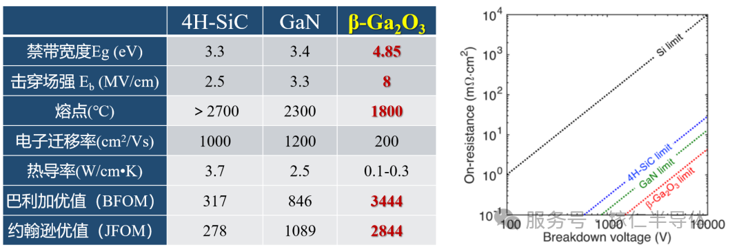
Figure 3. Physical property parameters of Gallium Oxide single crystal and reference diagram of Gallium Oxide power transistor
(Ref: S. J. Pearton, et al., Appl. Phys. Rev., 5, 2018, 011301; A. J. Green, et al., APL Mater., 10, 2022, 029201)
02 Gallium Oxide Has Broad Application Prospects
First of all, the application prospect of Gallium Oxide in the field of power devices is worth looking forward to, especially in the field of medium voltage, high voltage and UHV power devices greater than 650V, such as new energy vehicle fast charge, industrial power supplies, and high-voltage power modules for power grids.
Second, Gallium Oxide is also a potential substrate for high-power RF devices, such as communication base stations and radar systems.
Third, due to the application advantages of Gallium Oxide in deep ultraviolet optoelectronic devices, it can also be used in solar blind detection, radiation detection and other special fields.
If Gallium Oxide can be applied on a large scale in the future, our lives will change dramatically.
Taking new energy vehicles as an example, the use of Gallium Oxide power devices can help to increase the voltage of the high-voltage electrical system to 1200V or even higher. In the future, Gallium Oxide is expected to shorten the charging time of new energy vehicles to 1/4 of the present, achieving minut-level fast charging.
In addition, as a power electronic device, Silicon Carbide can be about 70% lower energy consumption than Silicon Carbide, and Gallium Oxide is 80% lower than Silicon Carbide power loss, so the application of Gallium Oxide will provide help for the goals of carbon peaking and carbon neutrality.
03 Gallium Oxide is Suitable for Large-Scale Industrialization
First, Gallium Oxide has significant industrial advantages in crystal growth. Similar to traditional semiconductor materials such as Si single crystal, Gallium Oxide single crystal can be grown by melt growth method, and is currently the only ultra-wide band gap semiconductor that can be grown by atmospheric pressure melt method. Compared with crystal growth methods such as vapor phase method, melt growth method is conducive to obtaining large size and high quality single crystal, and the crystal growth rate is fast and the efficiency is high. At the same time, it also has the advantages of low cost and large-scale production.
Secondly, Gallium Oxide is also suitable for industrialization in processing such as grinding and polishing. On the one hand, the hardness of Gallium Oxide (6) is close to that of Si single crystal (6.5), far less than that of Silicon Carbide (9.2), which reduces the processing difficulty, such as 8-inch Silicon Carbide cut takes about 200 hours, while the same size Gallium Oxide cut only takes about 20 hours, compared with 10 times the processing efficiency. Gallium Oxide, on the other hand, can be directly used silicon mature processing equipment technology, which reduces the Gallium Oxide on processing equipment research and development cycle and spending on research and development is conducive to the rapid industrialization of Gallium Oxide.
II Introduction to Casting Method
01 The Origin and Advantages of Casting Method
The casting method is a new melt growth method for the growth of Gallium Oxide single crystal, which is independently developed by the team of Academician Yang Deren of Zhejiang University. The casting method has the following significant advantages:
First, the casting method has low cost, because the amount and loss of precious metal Ir are significantly reduced compared with other methods, and the cost is significantly reduced.
Second, the casting method has high efficiency, the crystal growth rate of the casting method is fast (~100mm/h), and the thickness of a bulk is large (more than 20mm), so the bulk has a large amount of pieces and high production efficiency;
Third, the casting method is simple and controllable, and its process is short, high efficiency and easy to enlarge in size;
Fourth, the casting method has complete independent intellectual property rights, and the patents of China, Japan and the United States have been authorized, laying a solid foundation for breaking through the monopoly of foreign technology and realizing the substitution of localization.
02 Development of GAREN SEMI Casting Gallium Oxide Single Crystal
Since the establishment of GAREN SEMI company in 2022, the casting method Gallium Oxide single crystal size has achieved the rapid development of increasing the size of a generation every year, showing the technical strength of independent innovation. In May 2022, successfully grew 2 inches of Gallium Oxide single crystal; In May 2023, successfully grew 4 inches of Gallium Oxide single crystal; In February 2024, successfully grew 6 inches of Gallium Oxide single crystal; In February 2025, GAREN successfully grew an 8-inch Gallium Oxide single crystal.
03 The Casting Method Has Gradually Realized Industrialization and the Product Quality is Excellent
GAREN SEMI Gallium Oxide casting method has gradually realized industrialization, to provide downstream customers with large size and high quality Gallium Oxide single crystal substrate products. At present, GAREN SEMI’s 6-inch substrate has achieved product sales and shipments.
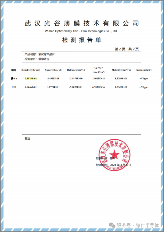
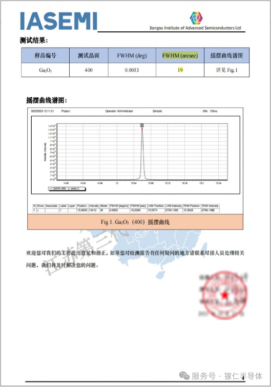
Figure 4 Third party test report of GAREN SEMI Gallium Oxide single crystal substrate products
(The figure above shows the electrical performance test results. The resistivity of conductive crystal is 25mΩ·cm and the concentration of carrier is 2.9×1018cm-1; the resistivity of UID crystal is 664mΩ·cm and the concentration of carrier is 6.9×1016cm-1; The image below shows the crystal quality test results, and the XRD half-height full width (FWHM) is 19arcsec.
Ⅲ GAREN SEMI Self-Developed Gallium Oxide Special
VB Crystal Growth Equipment is Fully Open for Sale
GAREN SEMI not only provides Gallium Oxide substrate products, but also fully open the sale of Gallium Oxide special VB crystal growth equipment and supporting process packages.
In September 2024, GAREN SEMI launched the first self-developed Gallium Oxide dedicated crystal growth equipment, which not only meets the high temperature and high oxygen environment requirements for Gallium Oxide growth, but also enables fully automated crystal growth, reducing manual intervention, and significantly improving production efficiency and crystal quality.
The equipment can obtain a variety of large size single crystal with different crystal faces through process control, and supports the upgrade to larger size single crystal to meet the needs of universities, scientific research institutes and enterprise customers for scientific research and production of Gallium Oxide crystal growth. The type of Gallium Oxide VB crystal growing equipment and its process package have been fully open for sale.
Company Profile
Hangzhou GAREN SEMI Co., LTD., founded in September 2022 and currently located in Xiaoshan District, Hangzhou, is a scientific and technological enterprise focusing on R&D, production and sales of Gallium Oxide and other wide-band gap semiconductor materials and equipment.
Relying on the National Key Laboratory of Silicon and Advanced Semiconductor Materials of Zhejiang University and ZJU-Hangzhou Global Scientific and Technological Innovation Center, the company has formed a R & D and production team with Yang Deren, academician of Chinese Academy of Sciences, as the chief consultant. The company research and development team created a new casting method Gallium Oxide single crystal growth technology, technological breakthroughs, the 8 inches single crystal growth is implemented in the industrialization of this technology to become an international first company, leading international dimension index; Achieved a technological breakthrough in the production of 3-inch wafer-grade (010) single crystal substrate, which is the largest size reported in the world at present; They independently developed special single crystal growth equipment for Gallium Oxide by VB method, which can not only meet the needs of high temperature and high oxygen environment for Gallium Oxide growth, but also carry out fully automatic crystal growth, which reduces manual intervention and significantly improves production efficiency and crystal quality.
Company has been approved by the National Technological SMEs, Zhejiang Province SNEs, Zhejiang Province Innovative SMEs, Zhejiang Province Technological SMEs, Hangzhou High-Tech Research and Development Center. The company has applied for more than 50 international and domestic invention patents, breaking through the monopoly and blockade of Western countries in Gallium Oxide single crystal materials.
The company's products include Gallium Oxide substrates of different sizes, crystal orientation and resistivity, and customizable Gallium Oxide seed crystals. The products are mainly used in power electronic devices for national grid, new energy vehicles, rail transit, 5G communication and other fields. After years of research, the company has mastered the core technology of the whole chain from equipment development, thermal field design, crystal growth, crystal processing, and can provide Gallium Oxide substrate with independent intellectual property rights. GAREN SEMI based on major national needs, continuous innovation in the upstream industry chain of Gallium Oxide, efforts to the development of power electronics industry in China for product security.
For more information about GAREN SEMI and its products
Please visit our official website: http://garen.cc/
Or contact us at:
Mr. Jiang :15918719807
Email :jiangjiwei@garen.cc
Mr. Xia :19011278792
Email :xianing@garen.cc