


News Trends
【World Express】Japan will Vigorously Promote the Development of Wide Band Gap Semiconductor Industry
日期:2023-03-14阅读:1374
Showa Electric began to produce SiC single crystal substrates internally, and strengthen the supply system of SiC epitaxial wafers (ingots on the left and SiC wafers on the right)
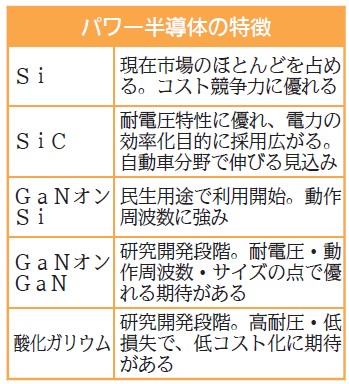
Power semiconductor has the function of changing voltage, frequency and converting power. The material technology crucial to these properties has begun to change. In new fields such as electric vehicles (EVs), the next generation materials are attracting people's attention as alternative for traditional silicon. New business opportunities are emerging to meet the demands of large current, high voltage and low power consumption. We have been following the trends of various companies aiming to achieve the growth of silicon carbide (SiC), gallium nitride (GaN) and other materials.
[Accelerating investment in SiC] NEDO-18.6 billion yen for supporting 8-inch R&D
"On-board power semiconductors are changing from silicon to SiC just like a black and white chess game," said president Hidehito Takahashi of Showa Denko K.K. about a year ago. Now, as the saying goes, the market is developing steadily, and semiconductor companies have accelerated their investment in SiC semiconductor.
Showa Denko K.K. is the world's largest supplier of homogeneous epitaxial wafers on SiC substrates. In recent years, it has signed a series of long-term supply contracts with Infineon Technology, ROHM and Toshiba Equipment&Storage. During the period of increasing consultation, the company also announced that it would start internal production of 6-inch SiC single crystal substrate in March. With external financing, the company will ensure stable supply of substrates and strengthen its SiC epitaxial wafer supply system.
Wafer is one of the most important materials in the semiconductor industry. The cultivation of SiC substrate manufacturers in Japan has also entered a new stage. The New Energy and Industrial Technology Development Organization (NEDO) has decided to provide about 18.6 billion yen to support the development of three research plans for 8-inch wafer technology, following the mainstream 6-inch wafer technology. Two companies, including Showa Denko K.K. and OXIDE, and Central Glass are taking new methods to ensure stable and high-quality single crystal mass production technology.
Central Glass uses solution method to grow crystals in silicon solution containing carbon. The solution method is characterized by no temperature change during crystallization and thermodynamic equilibrium. Compared with the traditional vapor phase method, it is easier to improve the crystal quality. It also makes it easier to lengthen the ingots, so that more wafers can be sliced more efficiently. While studying 8-inch technology, the company will "first establish 6-inch wafer mass production technology as soon as possible".
[Cost advantage of GaN on Si] Expectation of 5G and 6G applications
Gallium nitride on Silicon(GaN on Si) is a material grown by crystallization of GaN on substrate of Si.The characteristics of gallium nitride is suitable for high-frequency applications. The cost is expected to be reduced due to the widely used silicon substrate. In addition to EVs in major markets, it is expected to be adopted in the standard of the fifth generation communication (5G) and the next 6G communication. So far, products have been developed for medium voltage equipment in the range of several hundred volts.
For high voltage withstand, it is necessary to grow GaN layer with enough thickness on Si substrate. However, there are technical challenges in the production of GaN layers by chemical vapor deposition (CVD), such as substrate bending due to different thermal expansion coefficients.
In order to solve this problem, Chromis of the United States proposed a solution, namely QST substrate, which is a proprietary material that can inhibit bending during GaN deposition. Shin-Etsu Chemical has noticed this. It took over the technology of Chromis and began to commercialize the substrate materials by applying its own GaN on Si technology. The QST substrate has been specially improved to develop a substrate material that can be applied to power and high-frequency devices with withstand voltage above 1800 V. The company also produces and sells GaN deposited wafers through its subsidiaries, aiming to develop 12 inch wafers in the future.
[High performance GaN on GaN] Physical machinery and equipment will be put into use in 2022
Sumitomo Chemical, Mitsubishi Chemical Holdings and other companies will respectively operate the physical machinery and equipment for large size GaN single crystal substrate in 2022. The current GaN power semiconductor is made by growing GaN crystals on silicon substrate. Comparing with it, although it is still in the research and development stage, the growth of GaN crystals on GaN substrates is expected to help to produce power semiconductors with higher performance.
Masaki Matsui, director and senior executive director of Sumitomo Chemical, stressed that "GaN on GaN devices are expected to have more characteristics than other devices in terms of high voltage withstand, operating frequency and size". The development of element technology of GaN substrate has been basically completed, and the focus will be on improving production and productivity. The company will also be committed to enlarge new market for new equipment, with the goal of achieving real mass production in 2024.
Mitsubishi Chemical Holdings and Japan Steel Works have adopted the low-pressure acid ammonia heating method in their mass production demonstration equipment. GaN polycrystals were dissolved in supercritical ammonia and single crystals were redeposited. Northeastern University and Japan Steel Works jointly designed a hardener added to ammonia water, which can dissolve a large amount of ammonia water under lower pressure than traditional methods.
Gallium Oxide [Invented in Japan] is expected to be widely used in renewable energy, national defense and other fields
Gallium oxide (Ga2O3) is a material, whose epitaxial wafers, used in power devices for the first time in the world, are developed by research groups from the National Institute of Information and Communication Technology (NICT), Tokyo Agricultural and Industrial University, Tamura and other institutions.
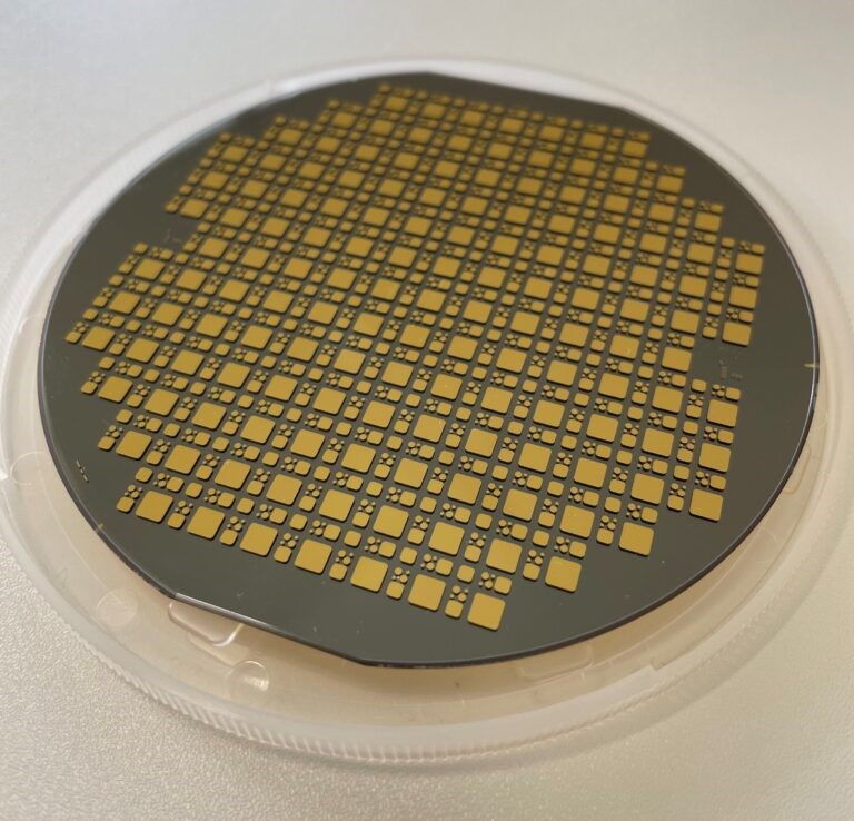
NCT gallium oxide epitaxial wafer (4 inches).
The melt method to grow single crystals has basically established the technology of effectively manufacturing substrates. Like other new materials, it is expected to reduce loss of the power conversion of equipment and therefor greatly reduce the cost. On the other hand, the structure of existing device needs to be modified on a large scale to achieve full performance.
"If the practical application makes progress, Ga2O3 will have the same or better characteristics as SiC. In the future, our goal is to replace SiC in the high-voltage field." Akito Kuramata,the president of NCT(Sayama, Saitama) stated their strategy. In addition to electric vehicles, the market is expected to be popularized in the fields of renewable energy and national defense.
"As a subsidiary of Tamura, NCT was established by transferring the technology of NICT. It sells substrates and wafers for research and development, and conducts technical research on improving output and film deposition efficiency. In terms of equipment development, “basic technology is in progress "(the president, Akito Kuramata,), and we plan to commercialize diodes and transistors. We are committed to popularizing materials invented in Japan in a large scale (ibid.) and making great efforts to improve the technology of mass production.
