


Member News
【Member News】Breaking the world’s highest performance of Gallium Oxide transistors – Adopts a new guard ring structure and demonstrates 3.2 times the performance of the power device compared to the previous record –
日期:2025-03-14阅读:1352
Novel Crystal Technology (NCT), a global leader in Gallium Oxide (Ga2O3) technology, has announced a successful development of a Gallium Oxide vertical MOS transistor (β-Ga2O3 MOSFET) with 1.23 GW/cm2 of the Power Figure of Merit (PFOM). This PFOM is the world’s highest value for β-Ga2O3 FETs and is 3.2 times higher than the previous highest value published by other research institutes. Part of this R&D effort was subsidized under the “Research and Development of Inversion-type channel Gallium Oxide MOS Transistors” program of the National Security Technology Research Promotion Fund (JP004596) of the Acquisition, Technology and Logistics Agency (ATLA) in Japan.
The results of this development will greatly advance the development of medium- to high-voltage (0.6–10 kV) gallium oxide transistors, which will lead to lower prices and higher performance of power electronics. In the future, the improvement of the efficiency and footprint of power electronic equipment such as industrial inverters and power supplies is expected to contribute to the electrification of the world, for instance electric vehicles, HVDC, and renewable energies such as solar and wind power which connect power systems to the grid. Details of these results was presented at the 72nd JSAP Spring Meeting on March 15, 2025, “Demonstration of β-Ga2O3 FinFET with power figure of merit of 1.23 GW/cm2 “.
1. Overview
Wide Bandgap materials, for example, Silicon Carbide (SiC)*1 and Gallium Nitride (GaN)*2 are under development to replace Silicon (Si) power devices*3. Gallium Oxide (β-Ga2O3)*4 has even superior material properties, and cost is more competitive due to faster crystal growth speed. It is expected to be applied to various power electronic devices such as home appliances, industrial equipment, electric vehicles, trains, solar power generation, and wind power generation, because of its low-loss and low-cost characteristics. Therefore, R&D around Ga2O3 is accelerated at companies and research institutes in the world, to reduce the size and efficiency of electrical equipment.
NCT has been working on commercialization of β-Ga2O3 MOSFETs under the “Research and Development of 10 kV Class Gallium Oxide Trench MOSFETs” and “Research and Development of Inversion-type channel Gallium Oxide MOS Transistors” programs, since awarded the ATLA contract in 2019. This time, the world’s highest PFOM*5 for β-Ga2O3 MOSFETs, 1.23 GW/cm2 was achieved by incorporating a high-resistance guard ring structure*6 with Mg ion implantation at the edge of gate electrode in a drift layer. The accomplishment will greatly advance the development of medium- to high-voltage (0.6–10 kV) Gallium Oxide transistors, which will lead to lower prices and higher performance of power electronics.
2. Achievements
Although NCT has been developing β-Ga2O3 MOSFETs, material’s superior high breakdown electric field strength (6–8 MV/cm) has not been fully exploited, due to the high electric field at the edge of the gate electrode. In other materials, a p-type conductive layer*7 is used at the edge of the electrode to reduce the electric field, but for Gallium Oxide, the p-type conductive layer technology has not yet been established, and the same method could not be applied. Therefore, instead of the technically unestablished p-type conductive layer, NCT’s researchers used a high-resistance β-Ga2O3 layer for the guard ring, and Mg, an acceptor impurity*8 that forms a deep level, was added to the layer through ion implantation*9 and activation heat treatment*10 processes.
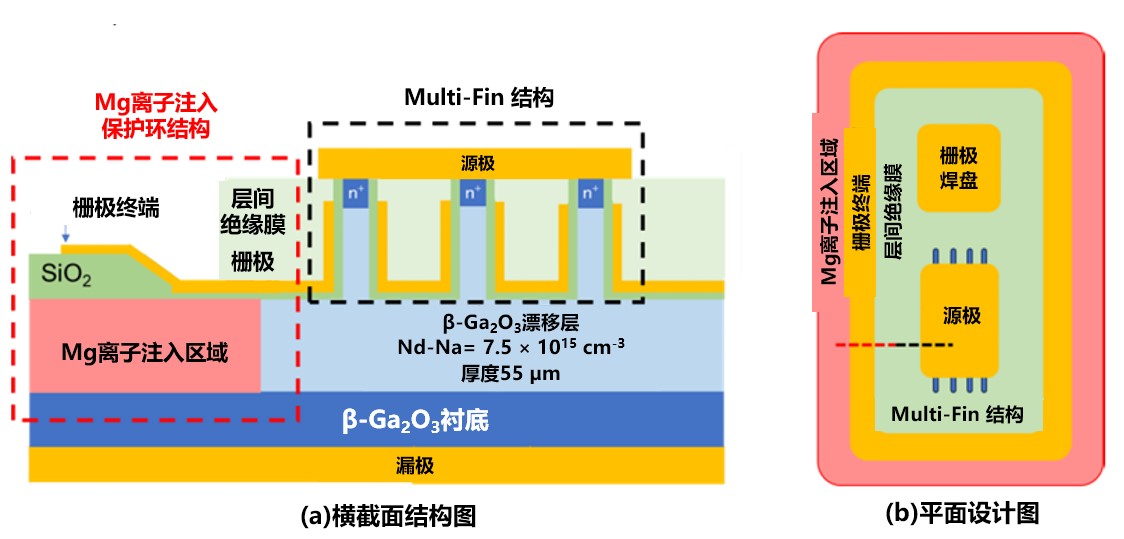
FIG. 1. Brief diagram of β-Ga2O3 MOSFET
Figure 1 shows the cross-sectional structure and plan view of the newly developed β-Ga2O3 MOSFET. The features of the transistor are as follows.
・Vertical device structure that is advantageous for low loss and high current required for power devices
・Multi-fin structure*11 with sub-micron mesa width channel that enable normally-off operation without a p-type
conductive layer
・β-Ga2O3 drift layer with a low donor concentration of 7.5×1015 cm-3, and a thick thickness of 55 μm.
・Guard-ring structure with Mg ion implantation to β-Ga2O3 in the area around the gate edge to reduce the electric field
at the region.
The prototype β-Ga2O3 MOSFET has 10 fins with a mesa width of 0.2 μm, a gate length of 3.5 μm, a fin length of 70 μm, and a fin pitch of 5 μm.
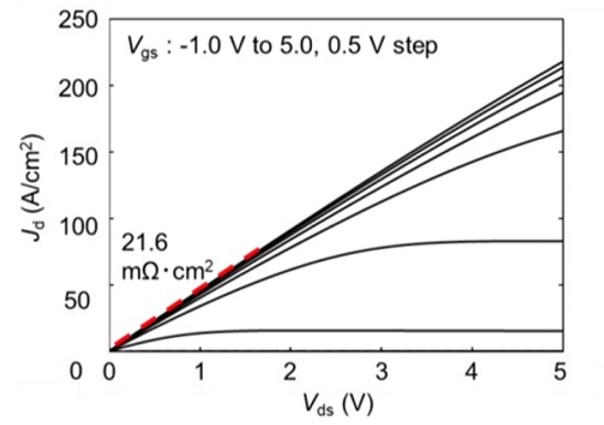
FIG. 2. Drain current-voltage characteristics
Figure 2 shows the drain current-voltage characteristics of a prototype β-Ga2O3 MOSFET. It exhibits normally off characteristics in which no current flows at gate voltage of 0 V. The maximum current density normalized by the source electrode area (50 μm × 60 μm) is 218 A/cm2, and the specific on-resistance is 21.6 mΩ·cm2 (Vgs = 5 V).
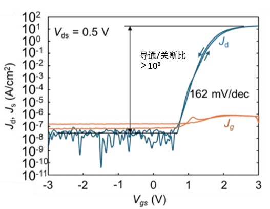
FIG. 3. Drain current · Gate current - Gate voltage characteristics
Figure 3 shows the dependence of the drain and gate currents on the gate voltage. The drain current on/off ratio is as large as 8 orders of magnitude or more, and the subthreshold slope*12 is 162 mV/decade, resulting in good transistor characteristics.
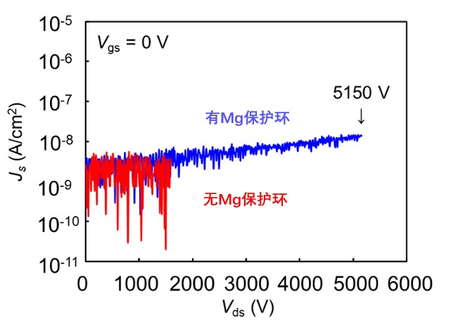 FIG. 4. Transistor withstand voltage waveform
Figure 4 shows the source and gate current characteristics when the gate voltage and source voltage are fixed at 0 V and a positive voltage is applied to the drain electrode. By applying a guard ring structure with Mg ion implantation, the breakdown voltage was increased from 1.6 kV to 5.15 kV. The maximum electric field strength in the β-Ga2O3 drift layer before and after the application of the guard ring structure is estimated to be 2 MV/cm and 3.72 MV/cm, respectively. NCT believes that the Mg guard ring reduces the concentration of the electric field at the gate electrode end and makes it possible to increase the electric field strength in the drift layer.
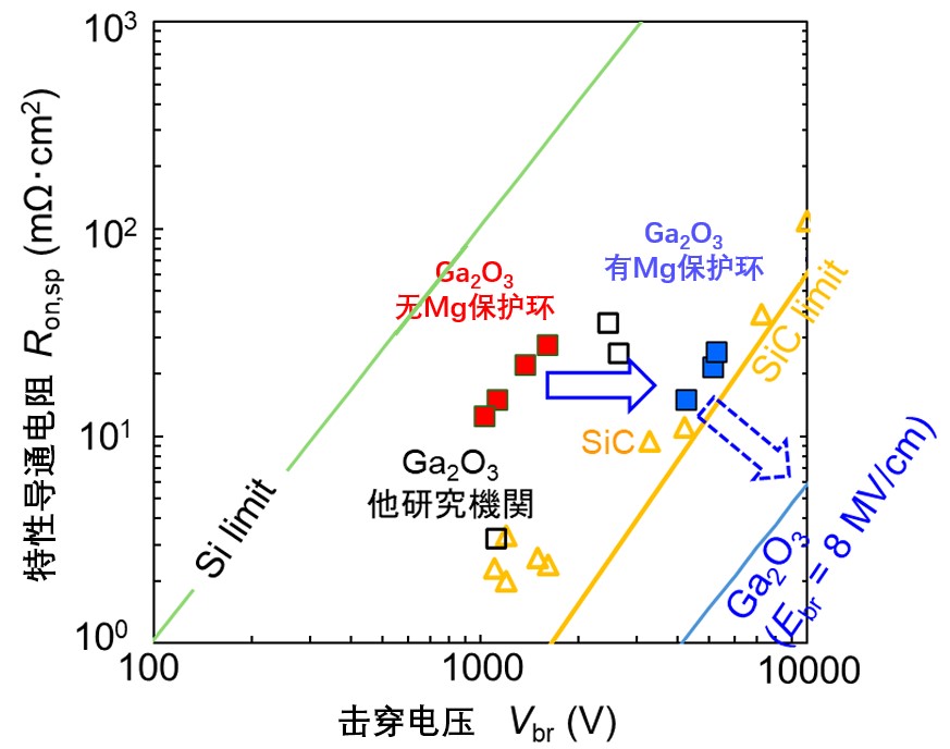
FIG. 5. Characteristic on-resistance and breakdown voltage of MOSFET
Figure 5 shows the relationship between the specific on-resistance (Ron, sp) and breakdown voltage (Vbr), which is a performance indicator of power devices. The breakdown voltage was greatly improved by incorporating a guard ring structure formed by ion implantation of Mg into β-Ga2O3 in the electrode termination region. As a result, it is 13.3 times more than before the application of the guard ring, a great PFOM value of 1.23 GW/cm2 was obtained. This PFOM value is the highest in the world for β-Ga2O3 FETs and is 3.2 times higher than the previous highest value for β-Ga2O3 FETs published by other research institutes.
3.What’s next
In the future, the researchers will further optimize the terminal structure of the β-Ga2O3 MOSFET, including the introduction of heterogeneous P-type semiconductor materials such as NiO, to further alleviate the problem of electric field concentration at the electrode termination. Through this technology, it is hoped that the high breakdown electric field strength (6~8 MV/cm) of β-Ga2O3 can be fully utilized to achieve high-performance Gallium Oxide power transistors beyond SiC.
The termination structure of β-Ga2O3 MOSFETs is further enhanced by utilizing hetero p-type semiconductor materials such as NiO, etc., to further reduce the electric field concentration at the electrode termination. NCT’s researchers aim to realize a β-Ga2O3 power transistor with performance exceeding that of SiC’s by exploiting the potential of β-Ga2O3‘s high breakdown field strength (6–8 MV/cm) with an advanced termination structure.
■Terminology
*1 Silicon Carbide (SiC)
It is a compound of silicon and carbon and is one of the wide-gap semiconductors.
*2 Gallium Nitride (GaN)
It is a compound of gallium and nitrogen and is one of the wide-gap semiconductors.
*3 Power device
It is a semiconductor device that can control voltage and current, and is used in power conversion equipment
such as inverters.
*4 Gallium Oxide (β-Ga2O3)
It is a compound of gallium and oxygen and is one of the wide-gap semiconductors.
*5 Power Figure of Merit (PFOM)
It is determined by VBR2/Ron,SP and is used to evaluate the performance of power devices. A higher number
indicates better performance.
*6 Guard ring structure
By arranging a conductive layer of a different type from the drift layer at the point where the electric field is
concentrated at the electrode termination, the equipotential surface is extended horizontally, and the electric field
concentration is relaxed.
*7 p-type conductive layer
In conductive semiconductors, the particles that carry the current are not electrons but holes.
*8 Acceptor impurity
It is an impurity in a semiconductor that captures electrons and negatively charges them. In general, by capturing
electrons, holes are generated in the semiconductor to form a p-type semiconductor.
*9 Ion implantation
It is one of the technologies for doping impurities to semiconductors. Impurity atoms are ionized and accelerated at
voltages of tens to hundreds of kV and driven into semiconductors.
*10 Activation heat treatment
It is a heat treatment to restore the damage suffered by the semiconductor during ion implantation and to promote
the electrical work of the injected impurities. Temperatures of 600–1200°C are usually used.
*11 Fin structure
This is the structure of the channel part of a MOS field-effect transistor, in which the gate is positioned on two sides
of the channel or wraps around the channel, forming a double gate structure. It is called a fin structure because it
has the shape of a fin (fish fin).
*12 Subthreshold slope
It is a performance index that indicates the off performance of the transistor, and is the gate voltage required to
increase the amount of current by an order of magnitude. It increases (deteriorates) depending on the quality of the
MOS interface.
