


Discover
【Knowledge Discover】Core Technology Affecting Semiconductor——Observation of Crystal from the Perspective of Symmetry (2)
日期:2025-03-18阅读:5254
Reading Guidance
Knowledge Discover is a new popular science column launched by the official account, focusing on in-depth analysis of cutting-edge materials and basic science. We will focus on the emerging semiconductor material of "Gallium Oxide", from crystal structure, physical properties to application scenarios, to comprehensively understand its breakthrough potential in fields such as 5G communication and new energy vehicles. At the same time, the column will also explore the scientific principles of Gallium Oxide materials and reveal their wide applications in energy, environmental protection, electronics and other fields.
In the previous article, we outlined the characteristics of various semiconductor crystals and their correlations from the perspective of crystal symmetry. This article will discuss the hexagonal and trigonal crystals based on HCP. We first describe the correspondence between hexagonal crystal system and trigonal crystal system, and outline the relationship between orthorhombic lattice and cubic lattice. We will then compare the details of HCP-based crystal structures from a symmetry point of view and explore the differences arising from defect.
Profile of Original Author

Hajime Okumura,Doctor of Engineering (Osaka University). Representative of Innovative Semiconductors, Electronics, & Energy Solutions, a limited liability partnership. Honorary Researcher of National Institute of Advanced Industrial Science and Technology. Honorary Associate Professor of University of Tsukuba.
Hexagonal and Trigonal Crystal Systems
The distinction between hexagonal and trigonal systems often causes confusion when discussing crystal systems. The essential difference between hexagonal and trigonal systems is the symmetry of the crystals, i.e. the hexagonal system has 6 axes of symmetry (rotation, inversion, helix), while the trigonal system has 3 axes of symmetry. In fact, the lattice structure of the two crystal systems is the same, as shown in Figure 2-1, the two-dimensional hexagonal net is stacked perpendicular to the plane, forming a hexagonal lattice (expressed in lattice constants as a = b ≠ c, α = β = 90°, γ = 120°). Since two rotations of 60° are equal to 120° rotations, the trigonal system appears to be contained in the hexagonal system (in fact, the two are the same when forming a lattice due to translational symmetry), but when the point group symmetry of the basic structure is set to a 3-fold rotation axis, the overall symmetry becomes a triple rotation axis. Figure 2-2 shows the symmetrical elements that appear in the hexagonal network when sextuple rotation axis and triple rotation axis are present on the lattice points of the hexagonal net. The difference in symmetry can be clearly seen from this figure. While the triple rotation axis of rotation appears in the basic cell at both (2/3, 1/3, 0) and (1/3, 2/3, 0) positions (shown in the red box), in (1) the double rotation axis in the center and side of the basic cell. In addition, the specular surface of the {1-10} faces have been added to (1).
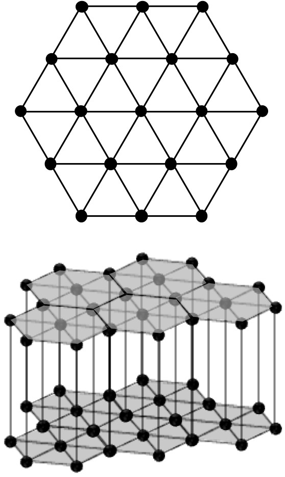
Figure 2-1 hexagonal net points and hexagonal lattice
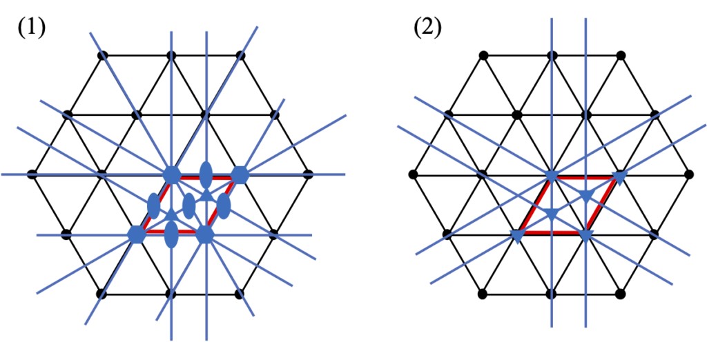
Figure 2-2 (1) Symmetry elements of hexagonal crystal system; (2) Symmetry elements of trigonal crystal system and hexagonal net The red box is the basic cell of the hexagonal net.
Now, let's revisit the relationship between the orthorhombic lattice, the hexagonal grid, and the HCP structure. Figure 2-3 shows the most densely packed arrangement of atoms in a common HCP structure. The thick black box is the basic cell of the basic hexagonal lattice. The black and red dots represent atoms. In this figure, the lattice points of the basic hexagonal lattice are defined as being in position to coincide with the atoms of the black dots. The locations of the red dots appear at first glance to be lattice points as well, but they are not. According to the definition of lattice points, integer multiples of the vectors connecting the lattice points between them (translation vectors) should also be translation vectors, but if the position of the red dot is also a lattice point, then the vector connecting the position of the black dot in the bottom left corner with the red dot, as shown by the red arrow in the figure, has no lattice point at double its position.
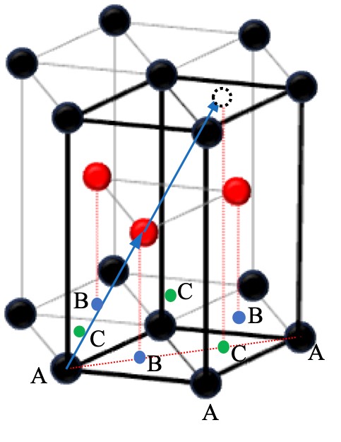
Figure 2-3 HCP structure. The bold black box is its basic cell.
So, if the positions of the red and white dots in Figure 2-3 are used as lattice points, what should the structure of the entire lattice look like? The result of the redrawing is shown in Figure 2-4 (1). In other words, if the positions of the blue arrows in Figure 2-3, and their double and triple positions, are taken as lattice points, and atoms are also placed at these positions, the translation symmetry can be coordinated. This lattice, as shown in Figure 2-4 (2) and (3), is a composite lattice consisting of three basic hexagonal lattices, called orthorhombic lattice. In this case, the spacing between layers (1/3 of the length of the C-axis) has no special restrictions on the lattice structure, only the position of the red dot within the a-b plane is important. The basic translation vector shown in Figure 2-4(4) can then be reconstructed by placing the three orthorhombic lattices rotated at 120° intervals in the normally drawn hexagonal prism. This is the basic trigonal lattice. That is to say, combining the sublattice obtained by translating the simple hexagonal lattice to (1/3, 1/3, 1/3) and (2/3, 2/3, 2/3) (taking the bottom left lattice point of Figure 2-4(3) as the origin) with it, the simple lattice reconstructed from the basic translation vector of the composite lattice is the simple trigonal lattice treated as a trigonal crystal system. A trigonal lattice can be represented by a hexagonal lattice, but not all structures represented by a hexagonal lattice can be represented by a trigonal lattice.
By now you may have noticed that the structure in Figure 2-4(2) is very similar to viewing the orientation of the FCC as the c axis in the <111> direction and stacking layers perpendicular to that plane. In fact, the simple cubic lattice, FCC, and BCC belonging to the cubic crystal system can all be regarded as a type of orthorhombic lattice, or more precisely, their fundamental translation vectors have a particularly high degree of symmetry (γ = 90°, 60°, 109.47°) in the trigonal lattice (lattice constants a = b = c, α = β = γ). In this sense, when comparing stacked structures of atomic layers, cubic crystals can also be represented as hexagonal lattices, which is easier to understand. Especially for FCC, the basic translation vector length of the trigonal lattice is equal to the basic translation vector length of the original hexagonal grid, and the three black dots on the bottom of Figure 2-4(3) and the red dots directly above it form a regular tetrahedral structure. In the future, when investigating the accumulation of the crystal structure as the densest accumulation layer, we correspond the <111> direction of the cubic crystal to the <0001> direction of the hexagonal crystal, and in the plane perpendicular to the C-axis of the hexagonal lattice, according to the relationship between upper and lower levels, the possible sites of the closest packing of atoms are labeled as sites A, B and c, as shown in Figure 2-4.
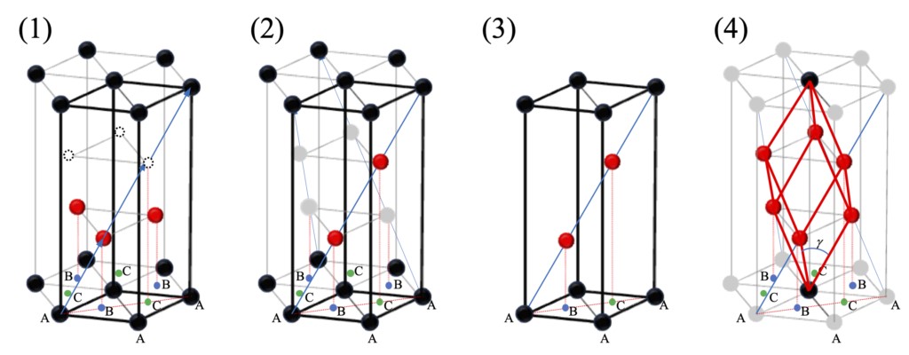
Figure 2-4 The relationship between hexagonal lattice and orthorhombic lattice drawn on the basis of hexagonal prism, (1) simple hexagonal lattice, (2) orthorhombic lattice (compound hexagonal lattice), (3) only the cells of (2) are taken out, and (4) the three orthorhombic lattices are reconstructed as the base trigonal lattice. In (2), (3) and (4), the locations of the atoms in the black and red circles are the lattice points. The symbols A, B, and C in the figure represent locations in the plane perpendicular to the C-axis where it is possible for the atoms to be closely packed between the upper and lower layers. In (4), when γ = 90˚, 60˚, and 109.47˚ (depending on the C-axis length), the lattices are simple cubic, FCC, and BCC lattices, respectively.
Hcp-Based Semiconductor Crystals (GaN, SiC, etc.)
Looking back at the development of semiconductor material technology, until around 1990, cubic crystals such as Si and GaAs were still the dominant technology. At that time, the understanding was that crystals other than cubic crystals could not be practical applications as semiconductors. The development of hexagonal semiconductor crystal technology such as GaN and SiC upended this common sense.
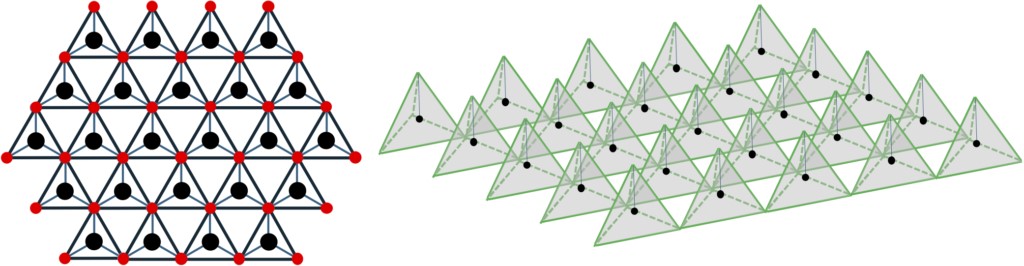
Figure 2-5 Layer structure with the regular tetrahedron structure with the atoms at the center of gravity in a two-dimensional way in the closest packed configuration. The diagram on the left is a floor plan. The picture on the right is a top view.
In HCP-based semiconductor crystals, as in FCC-based crystals, tetrahedral structures are also fundamental to forming crystals. When considering a two-dimensional structure with the closest packed configuration of atoms arranged in a tetrahedral structure at the center of gravity (refer to Figure 2-5) and stacked in sequence along the c-axis, if the closest packed site of the central atom is set as point A, the closest packed point B or C of the upper atoms can be configured. It can be seen that when this position is arranged in the direction of the C-axis, the stacking mode is ABCABC in the case of FCC based zincblende type (GaAs) and ABAB in the case of HCP-based wurtzite type (GaN). As shown in Figure 2-6, the stacked layer is the closest packed structure, and the layer containing different atoms in the holes between the upper layer is considered here. The basic unit cell of the hexagonal lattice is represented by the solid black line in the figure, which also shows the structure of the element consisting of the lattice atom 1 and the atom 2 located in the void. From the plane inside the unit cell of the figure, the position of atom 1 corresponds to point A, the position of atom 2 corresponds to point B, and the position of the void at the top right of atom 2 corresponds to point C.
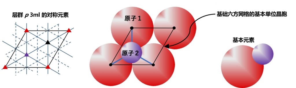
Figure 2-6 Basic hexagonal reticular monocytes and the basic elements in the closest packed. Atomic bonds are represented by blue lines. In addition, there is another atomic bond from atom 1 to the back of the graph and from atom 2 to the front of the graph. The symmetric elements of the layer group (p 3m1) to which the layer structure belongs are shown on the left. In the left image, the position of the red triangle corresponds to point A, the position of the purple triangle corresponds to point B, and the position of the non-atomic black triangle corresponds to point C.
Now, let's stack the layers in Figure 2-6 along the C-axis perpendicular to the surface of the paper. Due to the constraints of the bonding orientation, the layers need to be moved parallel to each other. In this case, atom 1 can only be placed on point B in layer 2 above layer 1. Further, in layer 3, the atom will be placed on point C. This arrangement, known as the "ABCABC" arrangement, is typical of zincblende structures. This stacking situation means that the lattice of layer 1 is stacked in a (1/3, 1/3) translation pattern within the layer. At the same time, this translation adds another 1/3 in the direction of the C-axis, thus forming a translation vector of (1/3, 1/3, 1/3) in space. This actually reflects the formation of the rhombic lattice. The formation of this rhombic lattice is due to the properties of the closest packed structure, where the three translation vectors have equal lengths and the angle between the vectors is 60˚. This geometric relationship determines that the rhombic lattice can be classified as FCC (face-centered cubic) structure.
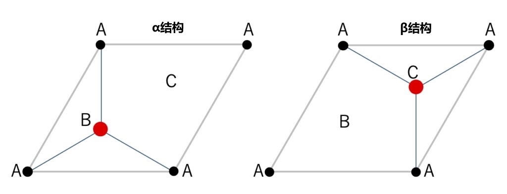
Figures 2-7 Include a schematic of the two-dimensional close-packed structure of the element structure, with its 180˚ rotation (both belonging to layer group p 3m1). The structure in the left image is an α structure, and the structure in the right image is a β structure.
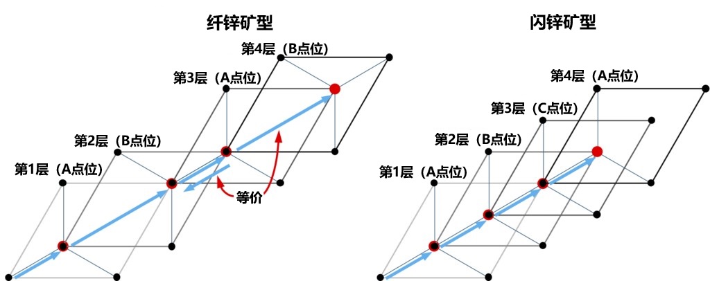
Figure 2-8 The stacking of two-dimensional close-packed structures including the element structure in the direction of the C-axis, with the in-plane movement direction [-1010] (the blue arrow in the upper right corner corresponds to the positive direction in the Zhdanov symbol). In the zincblende type, all layers move regularly (1/3, 1/3) through the α structure (1/3, 1/3), while in the wurtzite type, the α and β structures are alternately stacked, being (1/3, 1/3) in α→β and (2/3, 2/3) in β→α (equivalent to (-1/3, -1/3) in β→α).
As described above, only FCC structures can be generated when stacking only by moving the closest packed in parallel. Then, for how to construct the HCP structure, as shown in Figure 2-7, it is necessary to alternately stack the original closest packed layer with its 180° rotation (since the layer has a triple rotation axis, a rotation of 60° or 300° is geometrically equivalent). In the closest packed containing the basic elements shown on the right of Figure 2-6, there is no symmetric operation of double rotation axis or sextuple rotation axis, so the two layer structures in Figure 2-7 cannot be overlaps just by parallel movement. This means that when stacking the second layer, it is not only necessary to adjust the position of the lattice points, but also to rotate the entire layer by 180°. Figure 2-8 shows the process of stacking the two layer structures alternately. In addition, the 180° rotation of the layers can be clearly seen when looking at a crystal composed of regular tetrahedral arrangements from the <11-20> direction (Figure 2-9). Refer to these two layer structures as α and β structures, respectively. Both the α structure and the β structure have a unique location of the lattice points on the upper layer depends on the position of the atom 2 in its own layer. This means that in the stacking process, the arrangement order of the lattice points and the layer structure are closely related. In other words, above the base layer, the stacking order of the α structure is A→B→C→A→, while the stacking order of the β structure is A→C→B→A→. For FCC (zincblende type) structure, the stack is only composed of α structure, A, B, C three kinds of lattice points in 1/3 proportion order evenly arranged; The formation of HCP (wurtzite type) structure requires alternating arrangement of α structure and β structure. If the sequence and layer structure are represented as a whole, FCC can be described as "ABCABC..." , while HCP can be described as "AB'AB'" (where the 「'」 represents the β structure). This way of formulation is easier to understand. But in HCP, the translational symmetry between the adjacent layers is lost, and the lattice points correspond to the structure one by one. In a stack of regular tetrahedral layers, the key is where and how often the transformation takes place. Also, in HCP, point C is in a vacant state, so it is no longer equivalent to points A and B. This situation constitutes the main difference between the crystal structure of the FCC and HCP.
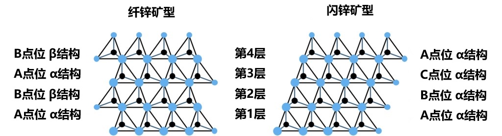
Figure 2-9 The arrangement of tetrahedral structures in wurtzite and zincblende structures from the hexagonal lattice - <1120> direction. The figure shows the site location and layer structure of each layer.
Next, we compare the symmetry of the {111} face of the stacked zincblende crystal and the {0001} face of the wurtzite crystal from the vertical direction. The closest packing positions and main symmetry elements of the two structures are shown in Figure 2-10. In the basic hexagonal lattice, the lattice point positions (point A) both have a triple axis of rotation. However, for points B and C, there are significant differences between the two structures. In zincblende type crystals, triple rotation axes exist at both B and C points; In wurtzite type crystals, point B has a triple rotation axis, but position C (where no atoms are present) forms a sextuple spiral axis with 63. Furthermore, in zincblende type crystals, there are three types of the closest packed positions, and correspondingly, the triple spiral axis regularly occurs in the unit cell surrounding these three closest packed positions. In wurtzite crystals, however, three double spiral axes occur only around the B position. Through this comparison, it can be concluded that zincblende type crystals have higher symmetry than wurtzite crystals.
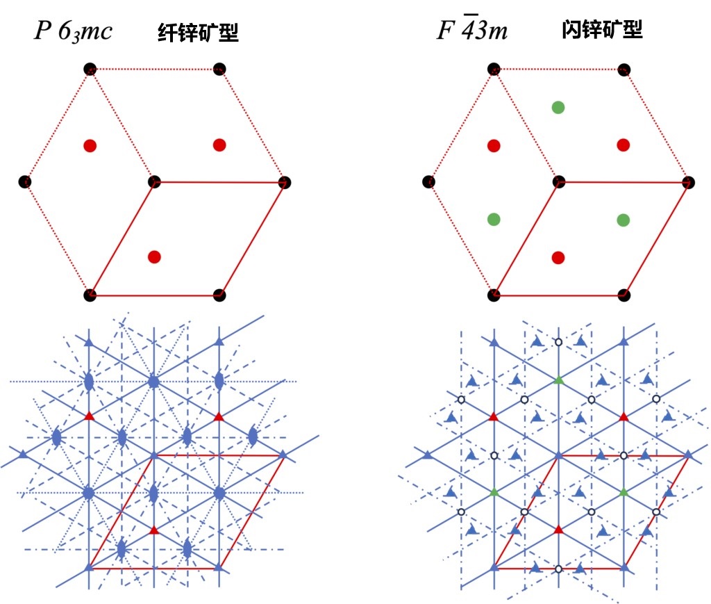
Figure 2-10 Atomic configuration and symmetry elements perpendicular to the wurtzite crystal {0001} face and zincblende crystal {111} face. The red box represents the unit cell in the hexagonal lattice, the black circle represents the atom at point A, the red circle represents the atom at point B, and the green circle represents the atom at point C.
After recognizing the difference, let's think about how the epitaxial film changes structurally as it passes from the base structure to the upper layer. As stated earlier, the regular tetrahedral structure, as well as the orientation of the chemical bonds, plays an important role in this. The binding states of the most surface atoms during growth are shown in Figure 2-11. As is well known in organic chemistry, the bonds between regular tetrahedrons formed by sp3 covalent bonds are considered more stable due to steric hindrance in the alpha arrangement shown in Figure 2-11. In the most surface layer, when the bonding direction of atom 2 is determined, the layer being formed above it is more likely to form an α arrangement. However, the orientation of the forming layer is not fixed because the bond of atom 1 extending upward has not yet been completed with the bond of atom 2 above it. In this case, the bond between the most surface atom 2 can be freely rotated as an axis, which is the mechanism by which the βstructure is generated during epitaxial growth. It can be considered that the structure formed by the more stable α structure arrangement is zincblende type structure, which is characterized by the regular arrangement of the three equivalent closest packed sites. In the wurtzite structure, however, because the C point is vacant, a crystal defect can occur if atoms enter here in a strange way. In addition, as a symmetric element at point C, the triple axis of rotation only completes the transfer of atomic arrangement information in this layer, while the sextuple helix axis is affected by the translation symmetry of the direction of the C-axis, and can only be true when the information of the upper and lower layers is accurately transferred. Epitaxial growth is the phenomenon that the structural information of the substrate is transmitted to the upper layer, but the longer the transmission distance to the upper layer which is forming, the higher the probability of natural errors will be. Further, if the regular tetrahedrons in the forming layer have bonded to each other to complete the formation of the layer, then the plane between atom 1 and atom 2 becomes the slip plane in the crystal. In this case, the presence of atoms at the C site, viewed from another Angle, is the same as the so-called "Shockley-Type Stacking Fault." From this point of view, in the wurtzite structure, some of the closest packed sites are vacant, and the rotational symmetry element present here is the spiral axis, so the possibility of C point atoms filling in the crystal growth process is high, which can be regarded as a growth error.
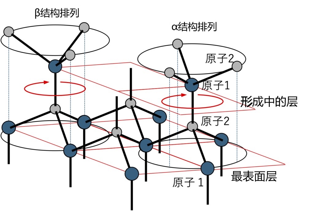
FIG. 2-11 Chemical bonding at the top surface of growth. The rotational motion shown by the arrows in the figure may occur in the cambium: in the β structure, the direction of bonding is rotated 180˚ with respect to the α structure; In the β structure, the position of atom 2 in the cambium overlaps the position of atom 1 in the topmost layer, but not in the alpha structure; In the alpha structure, the position of atom 1 in the cambium overlaps with the position of atom 2 in the topmost layer, but not in the beta structure.
Until now, we have considered the presence of atoms at point C in the HCP structure as an error that leads to a crystal defect. However, if in the stacked order of"ABAB", what happens if the atoms at point C appear in regular form? In fact, this phenomenon has actually been observed in the crystal polytype of SiC (Silicon Carbide) crystals. In SiC, representative crystal polytype include 4H, 6H, and 3C (according to Ramsdell notation). The stacked structure of these polytypes is shown in Figure 2-12. These stacks themselves are not specific to SiC, and the Zhdanov notation is handy for comparison purposes. For example, 3C is represented as (1) or (∞), 2H as (1-1), 4H as (2-2), and 6H as (3-3). In this notation, the number of stacks along the C-axis for the continuous α structure is represented by positive integers, the number of stacks for the continuous β structure is represented by negative integers, and the numbers in parentheses represent the repeating units. It is very intuitive to see the switching of layer structure at the junction of positive and negative integers. From the perspective of space groups, the space groups of 2H, 4H, and 6H are the same. However, from the perspective of layer to layer structure switching, 3C and 2H are at the two extremes, respectively, with some obvious regularity. In the 3C structure, the layer structure does not switch at all; In the 2H structure, each layer switches. The 4H and 6H structures are in between. In order to indicate the degree of switching, a concept called "Hexagonality" exists to quantify the frequency of switching between layers (50% for 4H and 33% for 6H).
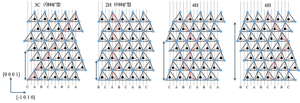
Figure 2-12 Layered structure (p3m1) periodically stacked crystal structure along the C-axis, where 3C is "ABCABCA...." 2H is "ABABA...." 4H is "CACBC...." 6H is "CABCBAC....". Here are the examples. In 2H, 4H, and 6H in the figure, point C has different characteristics than the other two sites. The red lines and hatchings are located in the same {11-20} plane. The arrows to the left of each figure indicate the C-axis length.
From the above Zhdanov notation, compared with 3C, the stacking structure of 2H, 4H and 6H can be understood as an "error" in the growth process, that is, the stacking structure is transformed during growth. This transformation occurs in a periodic form, such as every layer, every two layers, or every three layers. This periodicity in the C-axis direction must be maintained by crystal growth at the macroscopic scale, and the key mechanism for achieving this preservation is epitaxial growth. In epitaxial growth, information about the substrate needs to be accurately transmitted to the growing surface to ensure that the periodic structure can be faithfully reproduced. However, when the period in the C-axis direction becomes longer, the transmission of substrate information becomes difficult, resulting in the difficulty of accurately reproducing the stacked structure in the upper epitaxial layer. This means that the accuracy of information transmission and the stability of the growth process will be limited with the extension of the periodicity.
On the other hand, if the transformation of the layer structure is not periodic, then a local "stacking defect" can form. For example, in 4H-SiC crystals (Zhdanov denoted (2 2)), two typical stacking defects of "Single Shockley type" and "Double Shockley type" have been found to exist. These defects can be represented by (3-1) (ABA 'c '→ABCB') and (6-2) (ABA 'c 'aba 'c '→ ABCABCB' A '), respectively. These defects may be present in certain regions of the crystal in the direction of the C-axis, as they closely match the 4-layer period of the parent 4H-SiC. However, the 4H-SiC region above these stacked defects can cause stacking discontinuities due to the presence of defects, as shown in Figure 2-13. These defects will destroy the stacking regularity of the crystal, resulting in the loss of translational symmetry in the C-axis direction.
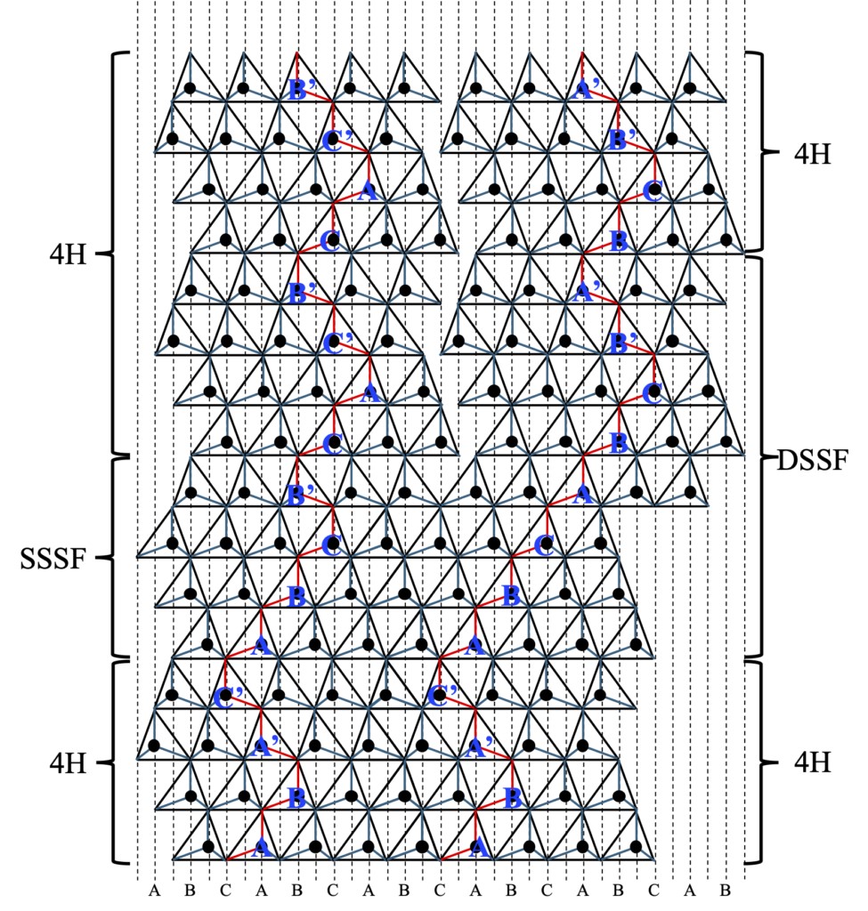
Figure 2-13 Stacking of Single Shockley Type Stacking Fault (SSSF) and Double Shockley Type Stacking Fault (DSSF) in 4H-SiC. The upper layer restores the periodic stacking structure of 4H-SiC, but the atoms occupy different sites than the bottom layer, and the stacking relationship between each other is irregular.
In this chapter, we have sorted out and analyzed the crystal characteristics and formation modes of HCP-based crystals, which are composed of the closest packed layers. In the next chapter, we will discuss the effect of the difference in the stacked structure on the crystal system, and the resulting tripartite rhombohedral lattice based crystals and monoclinic crystals.
References
Yasuyuki Kitano、Electronic Microscope, Vol.29, No.2, pp.118-123 (1994).
Appendix 2
· Representation of stacked structures
(1) Ramsdell notation: NSn
· N: The number of stacked layers in a period (i.e., cell).
· S: the symmetry of the cell (C: cubic, H: hexagonal, R: trigonal)
· N: If NS in the same group are the same, the serial number used as a distinction can be omitted.
(2) Zhdanov notation: (m-n.......)
· M: Number of stacked layers moving evenly in a positive direction
· -n: indicates the number of stacked layers that move evenly in the opposite direction
· .... : Repetition of different m-n pairs
· K: in the cell (m n.......) n The number of repetitions of the structure, omitted if 1.
· If k = 1 and the structure is clear, it can also be simply expressed as n.
(3) C-H sequence: c, h
A method of describing a single-period stacking structure in which the layer structure (α-structure or β-structure) is replaced by h (hexagonal) relative to the recently replaced layer and c (cubic) for the layer that is not replaced. For example, 3C is c, 2H is h, 4H is ch, and 6H is cch.
