Paper Sharing
【Domestic Papers】 University of Science and Technology of China --- Crystal-phase engineering of ε-Ga₂O₃ for high-performance deep UV photodetectors via MOCVD
日期:2025-03-20阅读:820
Researchers from the University of Science and Technology of China have published a dissertation titled "Crystal-phase engineering of ε-Ga2O3 for high-performance deep UV photodetectors via MOCVD" in Science China Materials.
Acknowledgement
This work was supported by the National Key Research and Development Program of China (2023YFB3610200 and 2024YFA1208800), the National Natural Science Foundation of China (61925110, U20A20207, 62304215, and 62171426), the University of Science and Technology of China (WK2100000025, YD2100002009, YD2100002010, and YD2100002007), the China Postdoctoral Science Foundation (2023M733367), and the CAS Project for Young Scientists in Basic Research (YSBR-029). This work was partially carried out at the Center for Micro and Nanoscale Research and Fabrication of the University of Science and Technology of China.
Abstract
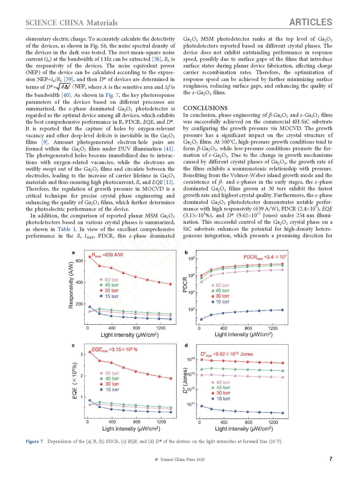
Gallium oxide (Ga2O3), with an ultrawide bandgap corresponding to the deep ultraviolet (DUV) spectra range, provides a potential subversive scheme for the filter-free DUV photodetection. Meanwhile, the various crystal phases of Ga2O3 provide more substrate options for achieving heteroepitaxy, with the coupling of Ga2O3 to SiC substrates conducive to developing integrated Ga2O3 DUV photodetectors. Phase engineering of β-Ga2O3 and ε-Ga2O3 was achieved on the commercial 4H-SiC substrate via metal-organic chemical vapor deposition. According to the in-depth analysis of different Ga2O3 growth stages, it was found that β-Ga2O3 is easy to form under high-pressure growth conditions, while low-pressure conditions promote the formation of ε-Ga2O3 at 500°C. Furthermore, the developed ε-phase dominated Ga2O3 DUV photodetector exhibits obvious advantages in high responsivity (∼639 A/W), photo-to-dark current ratio (∼2.4×10⁷), external quantum efficiency (∼3.15×10⁵%), and specific detectivity (∼9.62×10¹³ Jones) under 254 nm illumination. This work not only reveals the growth mechanism of Ga2O3 films under various pressures but also ensures the great potential of ε-Ga2O3 for highly sensitive DUV detection on the heterogeneous substrate, which is expected to expand the application of Ga2O3 optoelectronic devices.
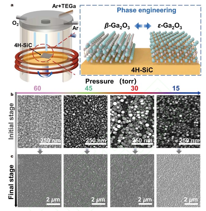
Figure1. Deposition and SEM characterization of the Ga2O3 films. (a) Schematic diagram of Ga2O3 heteroepitaxial growth on the 4H-SiC substrate via MOCVD. (b,c) Top-view SEM images of the representative Ga2O3 films grown under different growth conditions. The horizontal axis represents the chamber pressure during the growth process, while the vertical axis indicates the different growth stages: (b) the initial stage, and (c) the final stage. All the films were deposited at the same temperature (500°C).
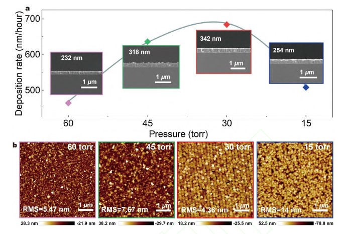
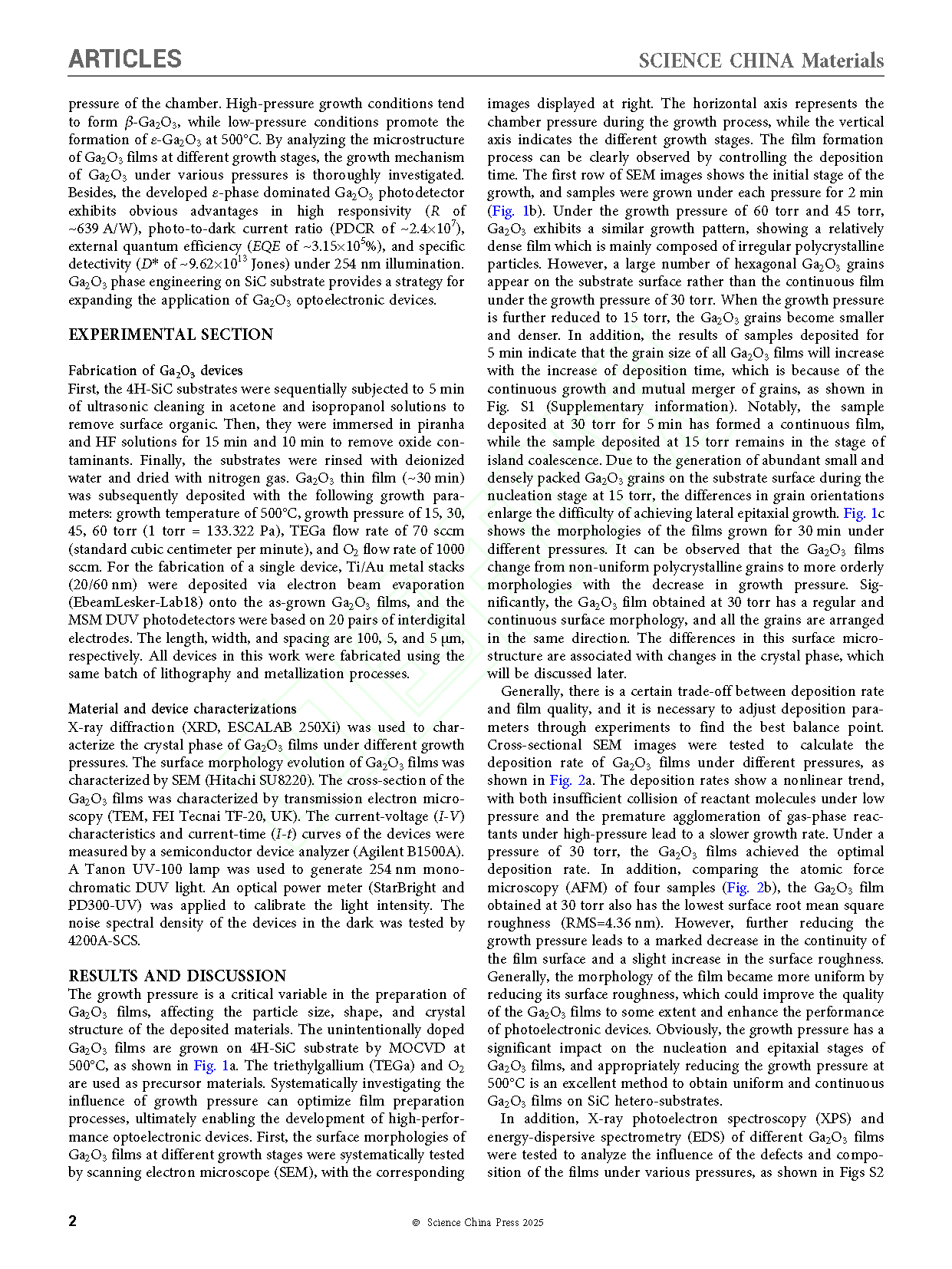
Figure 2. Deposition rate and AFM analysis of the Ga2O3 films. (a) Cross-sectional SEM images and deposition rate of the Ga pressures. (b) AFM images of the Ga2O3 films deposited under various pressures.
DOI:
doi.org/10.1007/s40843-024-3245-6