Paper Sharing
【Domestic Papers】Researchers Led by Academician Deren Yang from the Zhejiang University——Enhanced Emission in Erbium- and Ytterbium-Doped Gallium Oxide Devices with Constrained Energy Band on Silicon Substrates
日期:2025-03-24阅读:803
Researchers from the Zhejiang University have published a dissertation titled "Enhanced Emission in Erbium- and Ytterbium-Doped Gallium Oxide Devices with Constrained Energy Band on Silicon Substrates" in ACS Applied Electronic Materials.
Project Support
This work was supported by the Key Research Project of Zhejiang Province (Grant No. 2024C01054).
Background
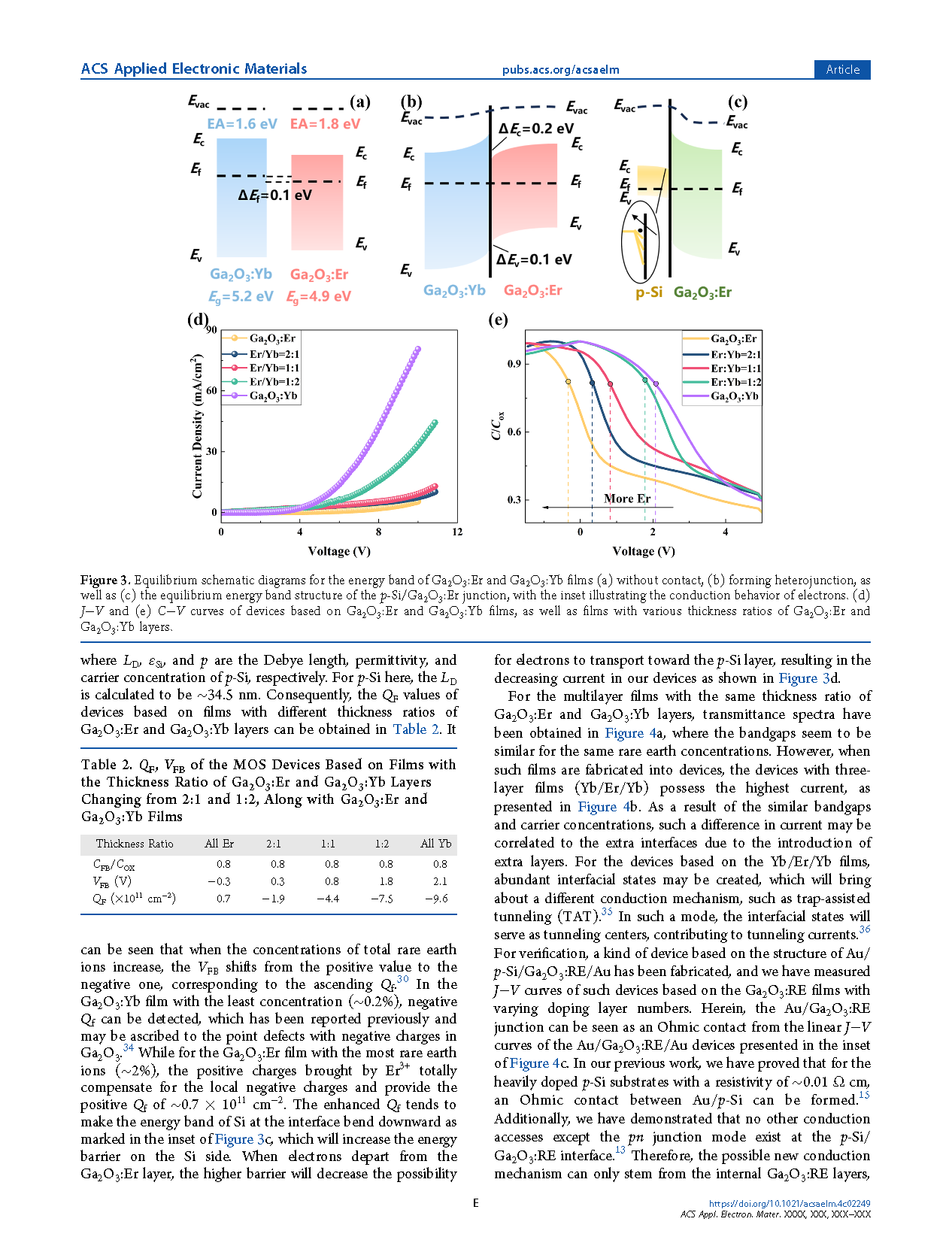
With the development of emerging semiconductor technology, the drawbacks of devices based on conventional electrical interconnection are becoming more and more apparent, such as signal delay, power consumption, and signal crosstalk. To address these issues, silicon-based optoelectronics have been proposed, where photons are expected to replace electrons for information transmission. However, to accomplish silicon based photonic circuits, electrically-driven light sources on silicon substrates are urgently needed. Nowadays, erbium ions (Er3+)-doped semiconductors have aroused extensive attention as candidates for light sources due to the merits of narrow spectral line width and the constant emission wavelength of the intra-4f transition between 4I13/2 and 4I15/2 (∼1.54 μm), which is located in the minimum-loss window of quartz fiber. Nevertheless, such emission faces the problem of low emission intensity limited by the concentration of sensitizers and the poor energy transfer efficiency.
Therefore, some external methods, such as adding other dopants or changing device structures, must be considered. For the method of doping, the energy transfer process might be disturbed by the extra energy levels brought about by the dopants. As a result, equivalent dopants that can serve as sensitizers for Er3+ emission are preferred. Among all trivalent elements, rare earth ytterbium ions (Yb3+) seem to be an ideal choice.
Abstract
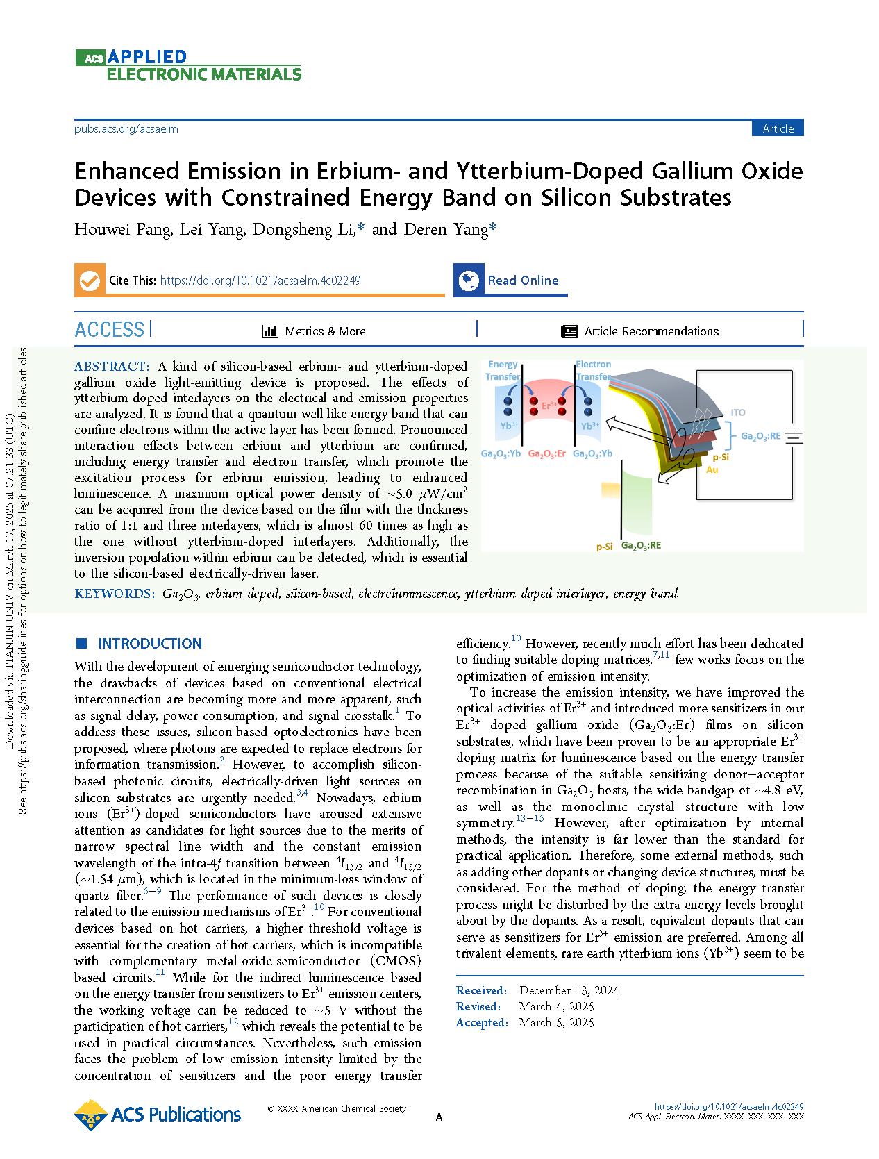
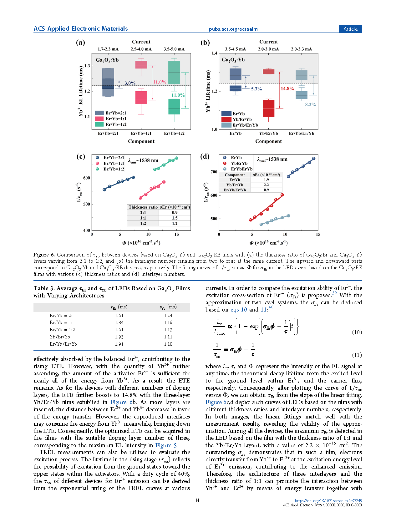
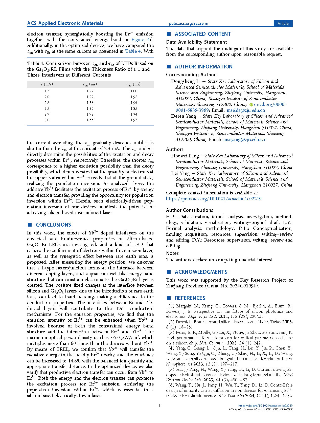
A kind of silicon-based erbium- and ytterbium-doped gallium oxide light-emitting device is proposed. The effects of ytterbium-doped interlayers on the electrical and emission properties are analyzed. It is found that a quantum well-like energy band that can confine electrons within the active layer has been formed. Pronounced interaction effects between erbium and ytterbium are confirmed, including energy transfer and electron transfer, which promote the excitation process for erbium emission, leading to enhanced luminescence. A maximum optical power density of ∼5.0 μW/cm2 can be acquired from the device based on the film with the thickness ratio of 1:1 and three interlayers, which is almost 60 times as high as the one without ytterbium-doped interlayers. Additionally, the inversion population within erbium can be detected, which is essential to the silicon-based electrically-driven laser.
Conclusion
In this work, the effects of Yb3+ doped interlayers on the electrical and luminescence properties of silicon-based Ga2O3:Er LEDs are investigated, and a kind of LED that utilizes the confinement of electrons within the emission layer, as well as the synergistic effect between rare earth ions, is proposed. After measuring the energy position, we discover that a I-type heterojunction forms at the interface between different doping layers, and a quantum well-like energy band structure that can constrain electrons to the Ga2O3:Er layer is created. The positive fixed charges at the interface between silicon and Ga2O3 layers, due to the introduction of rare earth ions, can lead to band bending, making a difference to the conduction properties. The interfaces between Er and Yb doped layers will contribute to the TAT conduction mechanisms. For the emission properties, we find that the emission intensity of Er3+ can be enhanced when Yb3+ is involved because of both the constrained energy band structure and the interaction between Er3+ and Yb3+. The maximum optical power density reaches ∼5.0 μW/cm2, which multiples more than 60 times than the devices without Yb3+. By means of TREL, we confirm that Yb3+ will transfer the radiative energy to the nearby Er3+ nearby, and the efficiency can be increased to 14.8% with the balanced ion quantity and appropriate transfer distance. In the optimized device, we also verify that productive electron transfer can occur from Yb3+ to Er3+. Both the energy and the electron transfer can promote the excitation process for Er3+ emission, achieving the population inversion within Er3+, which is essential to a silicon-based electrically-driven laser.
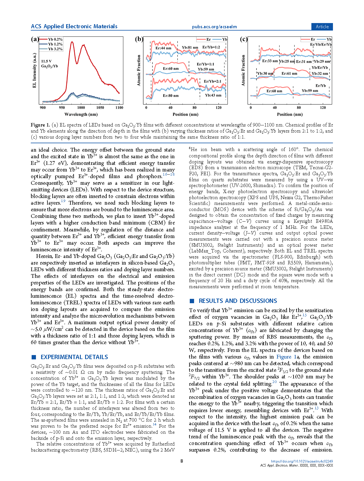
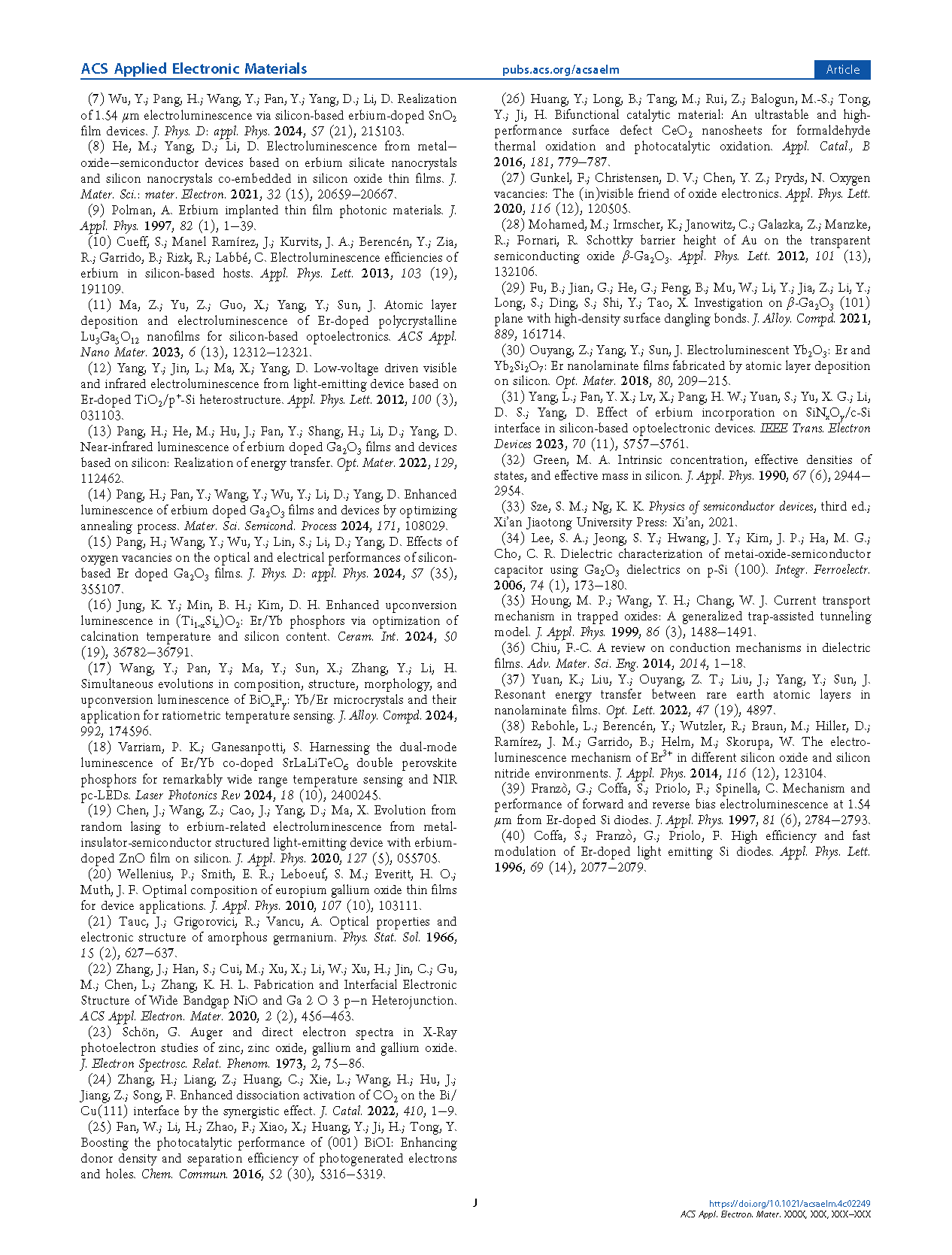
Figure 1. (a) EL spectra of LEDs based on Ga2O3:Yb films with different concentrations at wavelengths of 900−1100 nm. Chemical profiles of Er and Yb elements along the direction of depth in the films with (b) varying thickness ratios of Ga2O3:Er and Ga2O3:Yb layers from 2:1 to 1:2, and (c) various doping layer numbers from two to four while maintaining the same thickness ratio of 1:1.
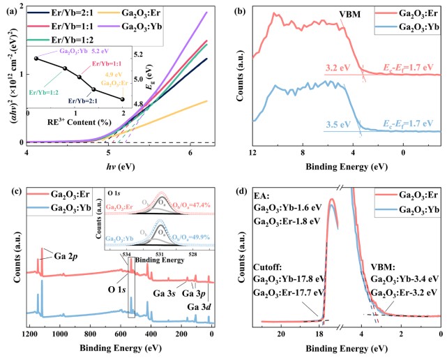
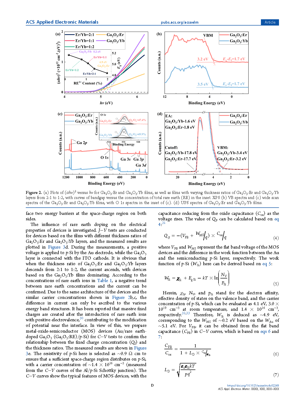
Figure 2. (a) Plots of (αhv)2 versus hv for Ga2O3:Er and Ga2O3:Yb films, as well as films with varying thickness ratios of Ga2O3:Er and Ga2O3:Yb layers from 2:1 to 1:2, with curves of bandgap versus the concentration of total rare earth (RE) in the inset. XPS (b) VB spectra and (c) wide scan spectra of the Ga2O3:Er and Ga2O3:Yb films, with O 1s spectra in the inset of (c). (d) UPS spectra of Ga2O3:Er and Ga2O3:Yb films.
DOI:
doi.org/10.1021/acsaelm.4c02249