Member News
【Member News】 8 Inches Gallium Oxide Wafer Substrate Shocked Appeared | Hangzhou GAREN Kernel Invite You to SEMICON Witness New Breakthrough in the Semiconductor Industry
日期:2025-03-26阅读:2283
On March 25, 2025, Hangzhou GAREN SEMI Co., LTD. (hereinafter referred to as "GAREN SEMI") made another breakthrough after releasing the world's first 8-inch Gallium Oxide single crystal, based on independent innovation Gallium Oxide single crystal growth technology and large size substrate processing technology, successfully prepared the world's first 8-inch (200mm) Gallium Oxide wafer substrate. China's fourth-generation semiconductor Gallium Oxide wafer substrate took the lead in entering the 8-inch era, not only filling the gap in the global Gallium Oxide industry, but also marking China's leap from following to leading in this field.

1、Significant Industry Value of 8-Inch Gallium Oxide Wafer Substrate
China's Gallium Oxide took the lead in entering the 8-inch era, and its industrial value can be reflected from three dimensions:
First, from the technical compatibility aspect. 8 inches Gallium Oxide substrate forms a good fit with the existing 8-inch manufacturing system of the silicon-based semiconductor industry, accelerating the industrialization process. This kind of production line compatibility advantage can effectively shorten the technology transformation cycle and reduce the cost of technology upgrading for enterprises.
Second, from the economic efficiency aspect. The significant increase in material utilization due to the upgrading of substrate size, the geometric increase in the number of chips that can be manufactured on a single wafer, and the optimization of the production process will drive a breakthrough reduction in the unit cost of Gallium Oxide devices and a significant increase in production efficiency.
Third, from the aspect of industrial strategy. China has taken the lead in overcoming 8-inch technical barriers to the preparation of Gallium Oxide in the world, which not only marks a major technological breakthrough in the field of ultra-wide band gap semiconductor in China, but also forms a moat of industrial competition through the establishment of first-mover advantages. This technology leapfrog for China's semiconductor industry to grasp the key voice in the global value chain reconstruction, and lay a solid foundation for the construction of an independent and controllable semiconductor industry ecology.
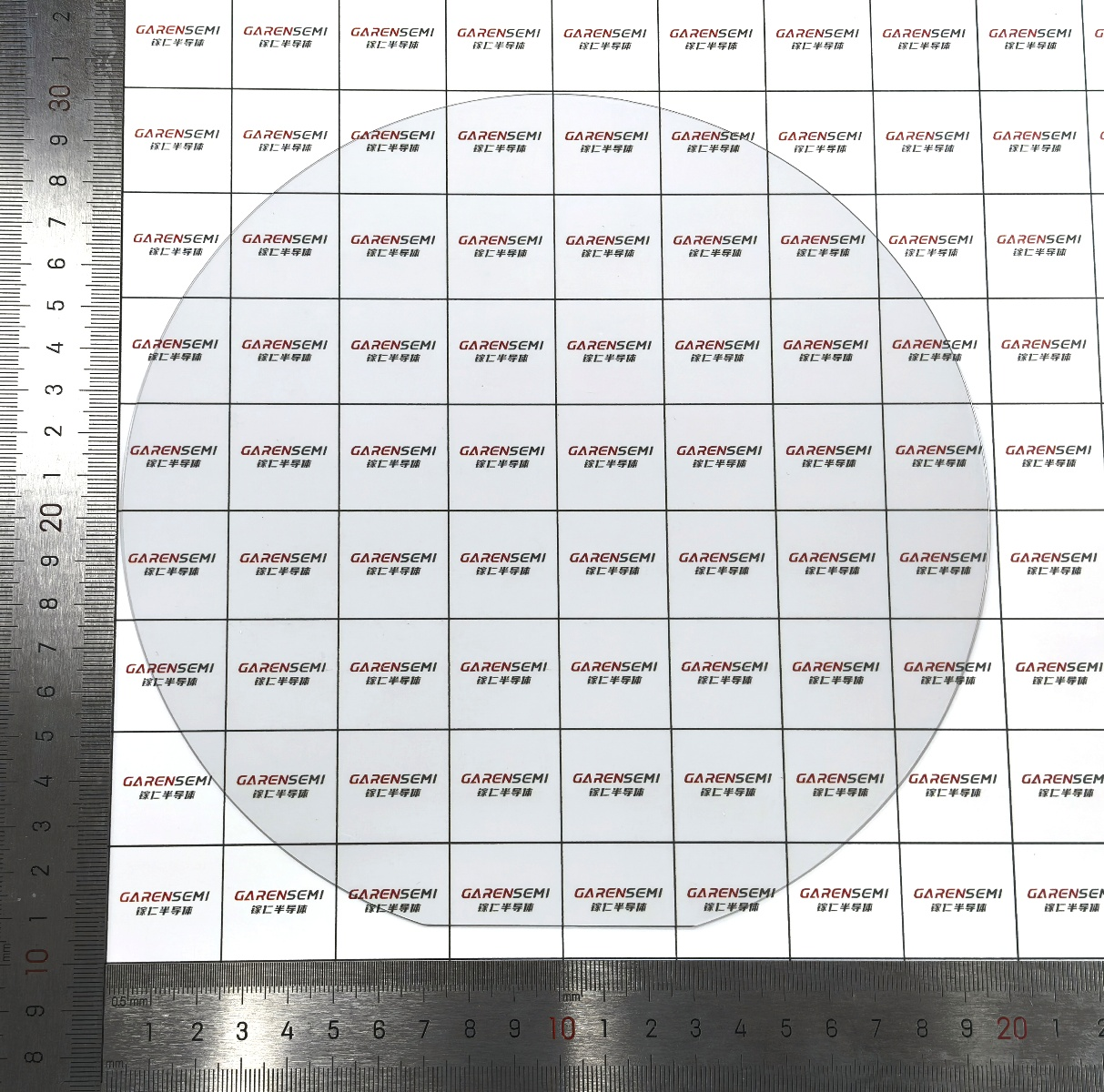
FIG. 1 GAREN SEMI 8-inch Gallium Oxide wafer substrate
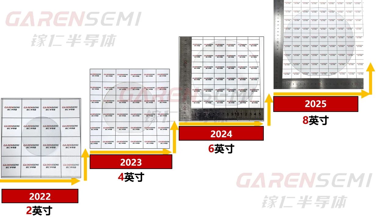
FIG. 2 Rapid evolution of GAREN SEMI Gallium Oxide wafer substrate size
2、Introduction to Gallium Oxide
In recent years, with the rapid development of new energy, photovoltaic power generation, radar detection, 5G mobile communication and other fields, ultra-wide band gap semiconductor materials with higher band-gap width and breakdown electric field strength represented by Gallium Oxide (β-Ga2O3) have attracted wide attention and attention from all circles.
Gallium Oxide Has Excellent Properties
① Higher Working Voltage and Power
The bandgap of Gallium Oxide single crystal is about 4.8eV, and the breakdown electric field strength is about 8 MV/cm, which is much higher than Si(1.1eV, 0.3MV/cm), SiC(3.3eV, 2.5MV/cm), GaN(3.4eV, 3.3MV/cm) and other materials. The produced power device has higher working voltage and power.
② Lower Energy Loss
The BFOM of Gallium Oxide is about 10 times that of SiC and 4 times that of GaN, and devices developed using Gallium Oxide will have smaller on-resistance and higher power conversion efficiency.
③ Meet Both High Frequency and High Power
Gallium Oxide has a large JFOM (2844), which has more advantages than SiC and GaN, and meets the requirements of high frequency and high power at the same time, and has a broad prospect in the RF field.
④ Excellent UV Photoelectric Performance
Gallium Oxide single crystal’s short UV cut-off edge (260 nm), and ultraviolet transmittance affected by carrier concentration is small, obvious advantages in preparation of deep ultraviolet electric parts.
⑤ Strong Thermal and Chemical Stability
Due to its excellent physical properties, Gallium Oxide has obvious advantages in the production of high voltage power devices, radio frequency devices, deep ultraviolet optoelectronics and so on.
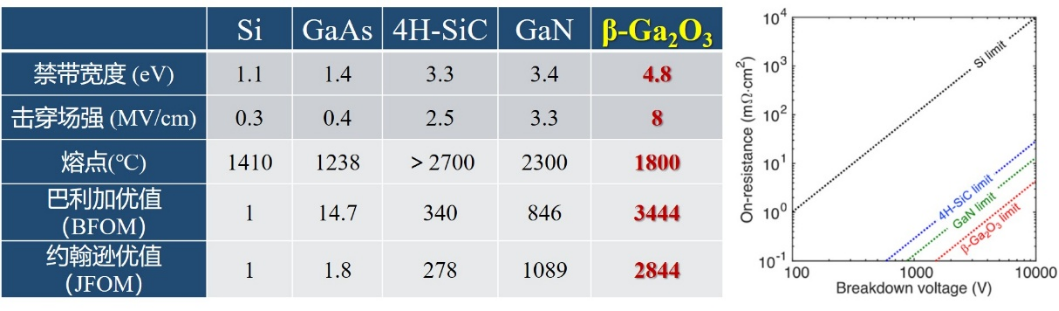
FIG. 3. Physical property parameters of Gallium Oxide single crystal and reference diagram of Gallium Oxide power transistor
(Ref: S. J. Pearton, et al., Appl. Phys. Rev., 5, 2018, 011301;A. J. Green, et al., APL Mater., 10, 2022, 029201)
Gallium Oxide Has Broad Application Prospects
① Power Device Field
Especially in the field of medium voltage, high voltage and UHV power devices greater than 650V, such as new energy vehicle fast charge, industrial power supply, power grid high voltage power module. At present, Gallium Oxide power devices mainly focus on Schottky diode (SBD) and field effect transistor (FET). Among them, the Gallium Oxide based SBD has faster switching speed, higher efficiency, better conductivity and high temperature operability. Gallium Oxide based MOSFETS can achieve fast switching between high current and high voltage while ensuring low loss. Taking new energy vehicles as an example, the use of Gallium Oxide power devices can help to increase the voltage of the high-voltage electrical system to 1200V or even higher. In the future, Gallium Oxide is expected to shorten the charging time of new energy vehicles to 1/4 of the present, achieving minut-level fast charging. In addition, as a power electronic device, the power loss of Gallium Oxide devices is much lower than that of silicon-based and Silicon Carbide devices, so the application of Gallium Oxide will provide support for the national dual-carbon strategy.
② The Field of High Power Radio Frequency Devices
Gallium Oxide has high electron saturation speed and JFOM, which has great application potential in the field of radio frequency devices, such as communication base stations and radar systems, and is of great significance for communications, national defense, aerospace and other fields. At present, the mainstream material for the production of RF devices is GaN, due to the expensive price of GaN substrate, the industry mainly uses Si, Sapphire, SiC substrate for heteroepitaxy to reduce costs, but since then there will be lattice mismatch between the substrate and epitaxy layer, resulting in a decline in quality. However, with the low lattice mismatch between Gallium Oxide and GaN, GaN epitaxy growth on Gallium Oxide as the substrate will improve the epitaxy quality. Therefore, Gallium Oxide has great potential in the RF field.
③ Deep Ultraviolet Optoelectronics Devices Field
Gallium Oxide can also be used in solar-blind detection, radiation detection and other special fields. "Solar-blind" ultraviolet detection is a new detection technology developed rapidly in recent years, mainly used in the military fields of ultraviolet early warning, ultraviolet reconnaissance, ultraviolet guidance and ultraviolet non-line-of-sight communication, as well as environmental monitoring, biochemical detection, industrial combustion process control, medical ultraviolet imaging and other civilian fields.
In the future, with the promotion and maturity of Gallium Oxide applications, it is also expected to be applied to frontier fields such as space technology, commercial aviation and low-altitude economy. In the future, the solar-blind characteristics, radiation resistance and extreme environment resistance of Gallium Oxide will be extended to the high-reliability electronic devices on space vehicles and other space science and technology fields, helping to improve the stability and life of space electronic systems. In commercial aviation, the high breakdown electric field strength and low on-resistance characteristics of Gallium Oxide make it suitable for the manufacture of power devices in avionics, which can enable lightweight and efficient aircraft power systems. Based on its photoelectric characteristics, Gallium Oxide can be made into a variety of sensors, which helps to improve the safety and maintenance efficiency of aircraft. For the booming low-altitude economy, its application potential in UAV ultra-fast charging modules and communication infrastructure is also worth looking forward to. At present, China has formed a full chain research and development system from crystal growth to device design. With the deepening of industry, education and research collaborative innovation and upstream and downstream linkage, this strategic new material may become a shining star in the wide band gap semiconductor family.
3、Meet in SEMICON Event
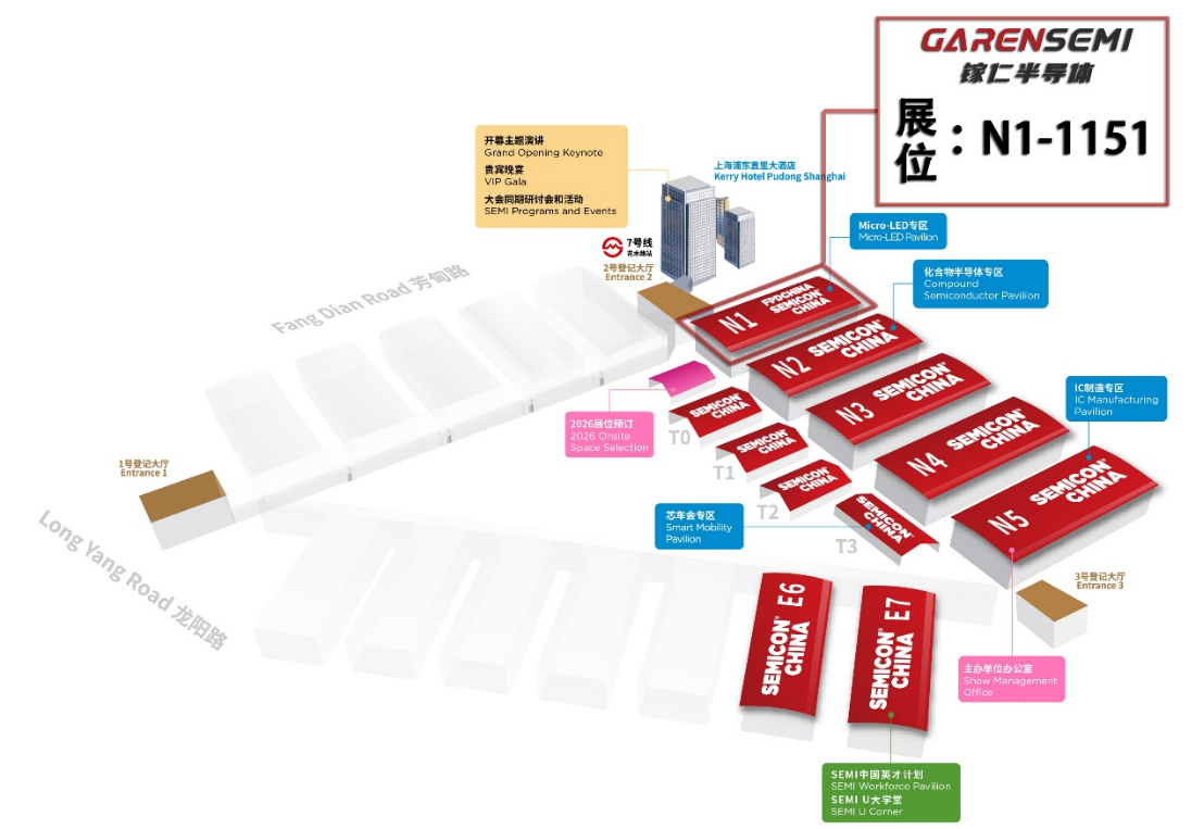
As SEMICON CHINA 2025 is being held at Shanghai New International Expo Center (No. 2345 Longyang Road, Pudong New Area, Shanghai), GAREN SEMI will attend the event and exhibit 8-inch Gallium Oxide wafer substrates. GAREN SEMI will be waiting for your visit at the scene to exchange industry trends, communicate the latest scientific research and technology, explore new ideas in the industry, develop new models, and seek new cooperation! We sincerely invite you to visit our booth N1-1151.
4、GAREN SEMI Self-Developed Gallium Oxide Special Productions
VB Crystal Growth Equipment is Fully Open for Sale
GAREN SEMI not only provides Gallium Oxide substrate products, but also fully open the sale of Gallium Oxide special VB crystal growth equipment and supporting process packages.
In September 2024, GAREN SEMI launched the first since the research Gallium Oxide semiconductor crystal growth equipment for special purpose, not only can satisfy the Gallium Oxide growth demand for high temperature and high oxygen environment, and can be fully automated crystal growth, reduces the artificial intervention, improve the production efficiency and improve the quality of crystal.
The equipment can obtain a variety of large size single crystal with different crystal face through process control, and supports the upgrade to larger size single crystal, to meet the needs of universities, scientific research institutes and enterprise customers for scientific research and production of crystal growth. The type of Gallium Oxide VB crystal growing equipment and its process package have been fully open for sale.
For more information about GAREN SEMI and its products
Please visit our official website: http://garen.cc/
Or contact us by:
Mr. Jiang :15918719807
Email :jiangjiwei@garen.cc
Mr. Xia :19011278792
Email :xianing@garen.cc