Paper Sharing
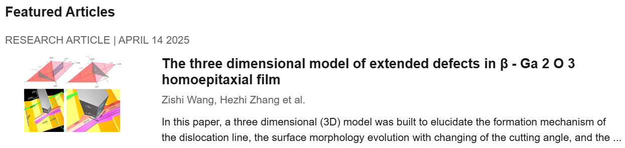
【Member Papers】Dalian University of Technology --- The three dimensional model of extended defects in β-Ga₂O₃ homoepitaxial film
日期:2025-04-17阅读:783
Researchers from the School of Integrated Circuits, Dalian University of Technology have published a dissertation titled "The three dimensional model of extended defects in β-Ga2O3 homoepitaxial film" in Applied Physics Letters. And has been chosen as the Featured Article.
Abstract
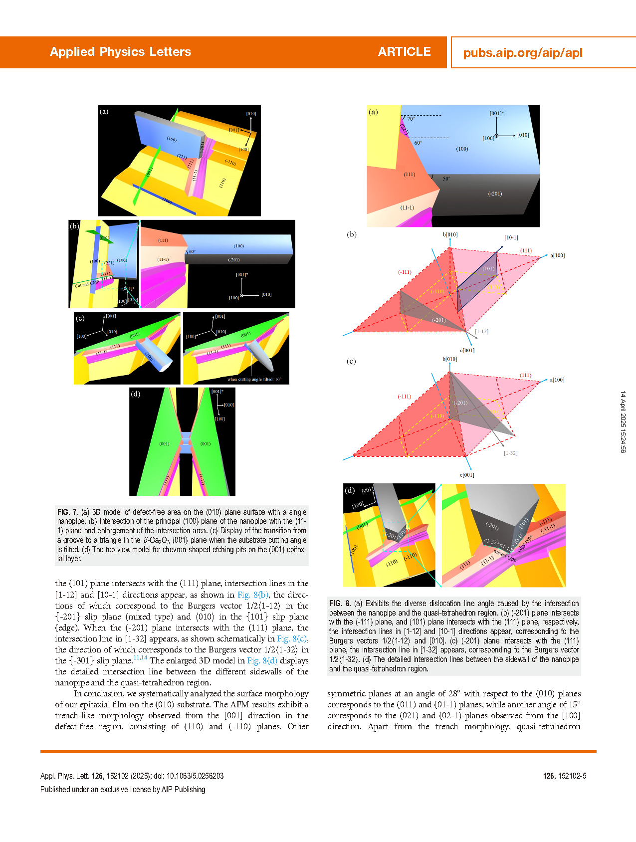
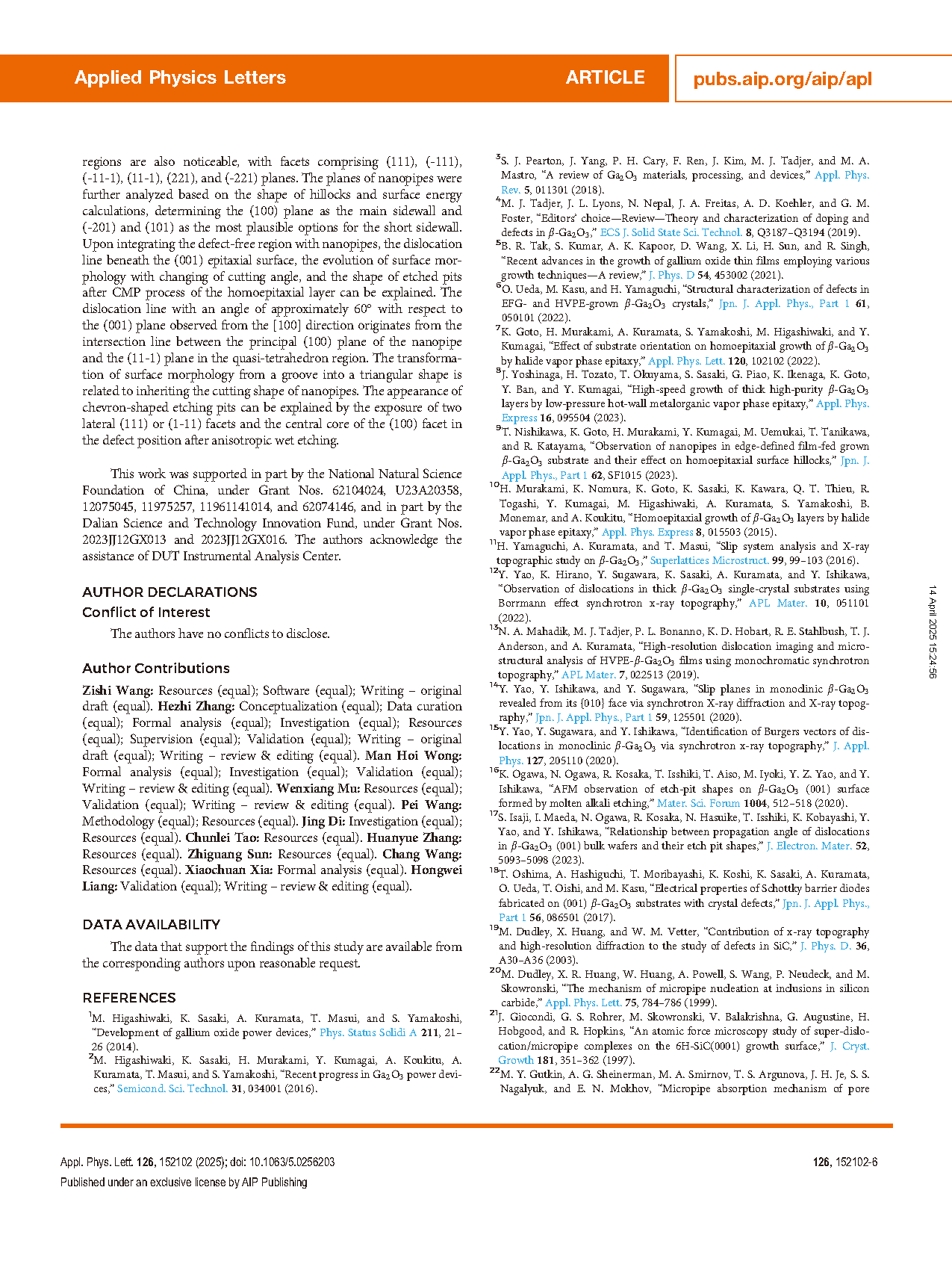
In this paper, a three dimensional (3D) model was built to elucidate the formation mechanism of the dislocation line, the surface morphology evolution with changing of the cutting angle, and the shape of etched pits after the chemical-mechanical polishing (CMP) process of a (001) homoepitaxial film. The dislocation line of an angle at approximately 60° with respect to the (001) plane observed from the [100] direction originates from the intersection line between the principal (100) plane of the nanopipe and the (11-1) plane in the quasi-tetrahedron region of the (010) plane surface. The surface morphology transition from a groove to a triangular pit is related to inheriting the cutting shape of nanopipes on the (001) surface. The appearance of chevron-shaped etching pits on CMP processed (001) homoepitaxial film can be explained by exposing two lateral (111) and (1-11) facets as sidewall, with the (100) facet remaining as the central core in the defect position after anisotropic wet etching. The 3D model also provides the possibility to explain the different angles and the Burgers vector of dislocation lines in single-crystal substrates, which is due to diverse sidewall planes of the nanopipe intersection with the planes in the quasi-tetrahedron region of the (010) plane.
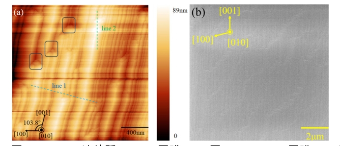
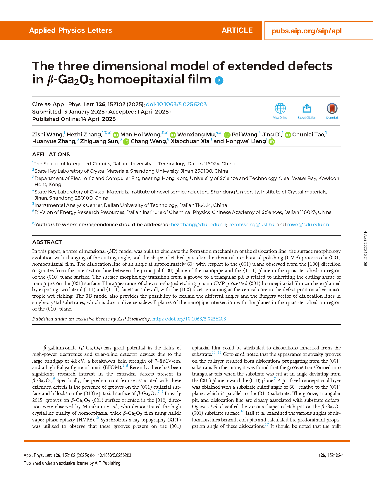
FIG.1 (a) AFM image of Ga2O3 thick film epitaxial by OVPE method; (b) SEM image of Ga2O3 thick film
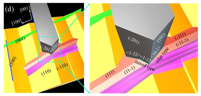
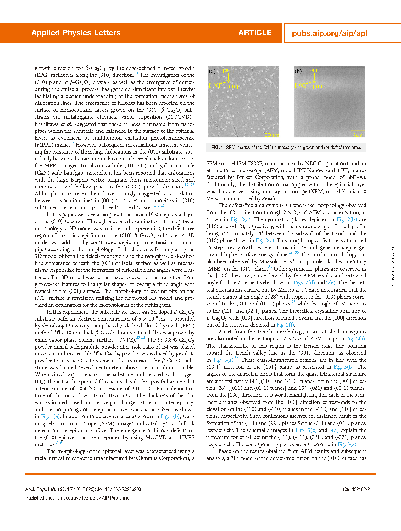
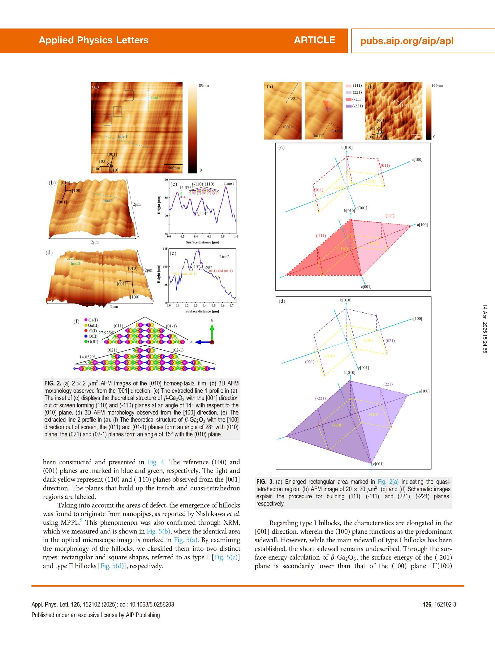
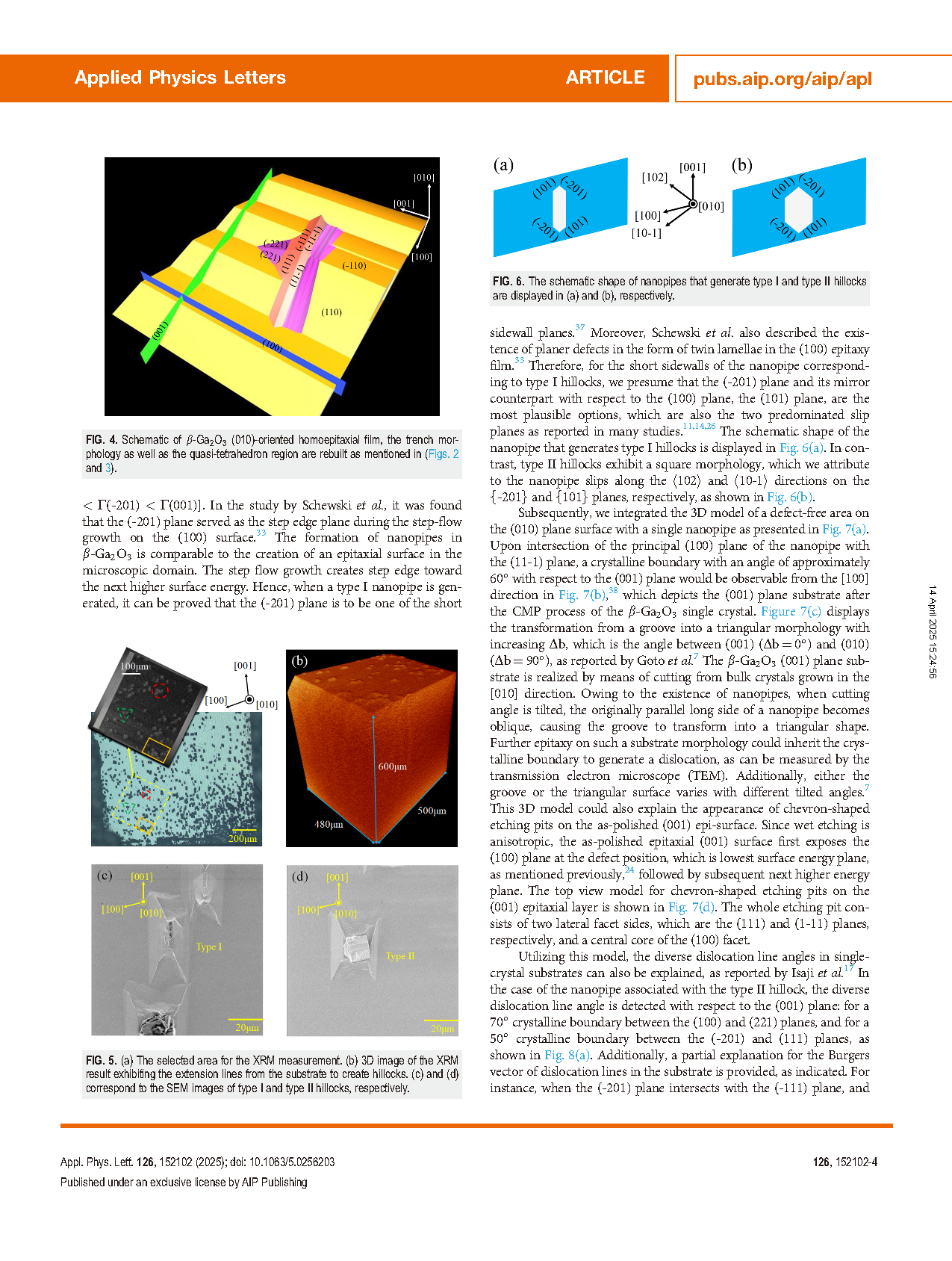
FIG.2 Three dimensional model diagram of directional dislocation lines formed
DOI:
doi.org/10.1063/5.0256203