Paper Sharing
【Member Papers】Xidian University --- 1.96 kV p-Cr₂O₃/β-Ga₂O₃ heterojunction diodes with an ideality factor of 1.07
日期:2025-04-17阅读:843
Researchers from the Xidian University have published a dissertation titled "1.96 kV p-Cr2O3/β-Ga2O3 heterojunction diodes with an ideality factor of 1.07" in Applied Physics Letters.
Project Support
We would like to thank the National Natural Science Foundation of China (NSFC) for their support and funding (Grant No. 62222407). This work was also supported by the Guangdong Basic and Applied Basic Research Foundation (Grant No. 2023B1515040024).
Background
Beta-gallium oxide (β-Ga2O3), with its ultra-wide bandgap (UWBG) of ~4.8 eV, high critical breakdown field (Ec) of 8 MV/cm, and significant Baliga’s figure of merit (BFOM) of 3200, along with controllable n-type doping concentrations, has emerged as a promising material for power semiconductor applications. It is theoretically poised to surpass silicon carbide (SiC) and gallium nitride (GaN) in performance. The ability to manufacture large-area native substrates using cost-effective crystal growth methods further enhances β-Ga2O3’s potential for future commercialization. However, the lack of p-type Ga2O3 has hindered the development of high-power bipolar devices, limiting the implementation of commercial deployment strategies. Devices based on p-type terminations generally rely on heterojunction (HJ) structures, with alternative p-type materials including Cu2O, NiO, IrOX, Cr2O3, and p-Si. Breakdown voltage (BVs) ranging from 1 kV to over 10 kV have been reported in Ga2O3 lateral and vertical diodes, as well as lateral MOSFETs. Among these, NiO has drawn considerable attention for its use in β-Ga2O3 diodes and MOSFETs due to its promising potential. However, its thermal stability remains a major challenge.
Abstract
In this Letter, we report on a p-Cr2O3/n-Ga2O3 vertical heterojunction diode (HJD) with a kilovolt-level breakdown voltage (BV). The chromium oxide (Cr2O3) film was deposited via magnetron sputtering, with a controlled thickness of approximately 20 nm and a hole concentration of 1 × 1016 cm−3. High-resolution transmission electron microscopy of the p-Cr2O3 film reveals a polycrystalline lattice structure. At room temperature, the 40 μm radius HJD exhibits a turn-on voltage (Von) of 1.7 V, a specific on-resistance (Ron, sp) of 4.6 mΩ·cm2, and a BV of 1.96 kV. Notably, the ideality factor (η) of the HJD is 1.07, the closest to 1 among all reported Ga2O3 HJDs, indicating a high-quality interface at the p-Cr2O3/n-Ga2O3 HJ. Additionally, the BVs at 75 and 150 °C are 1.63 and 1.4 kV, respectively, demonstrating the promising potential of p-Cr2O3/n-Ga2O3 HJDs for high-temperature and high-power applications.
Conclusion
In summary, we have fabricated p-Cr2O3/n-Ga2O3 HJDs with kilovolt-level BVs and an exceptionally low η\neth of 1.07. The 40μm radius diode achieved a P-FOM of 835 MW/cm2, with a Ron,sp of 4.6 mΩ·cm2, a BV of 1.96 kV, and a low IR < 10 μA/cm2. At 75 and 150 °C, the BV values were 1.63 and 1.40 kV, respectively. Outstanding HJ contact interface, crystalline material quality, and high-temperature reliability make p-Cr2O3 a promising material for Ga2O3-based medium-voltage and high-voltage devices.
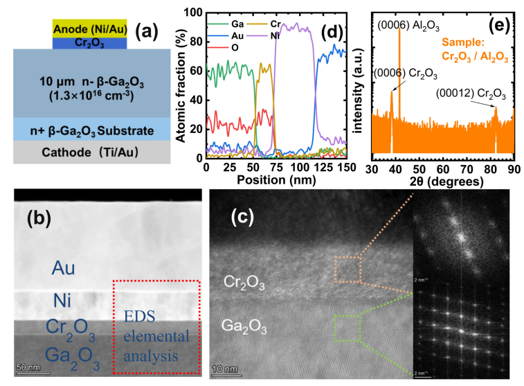
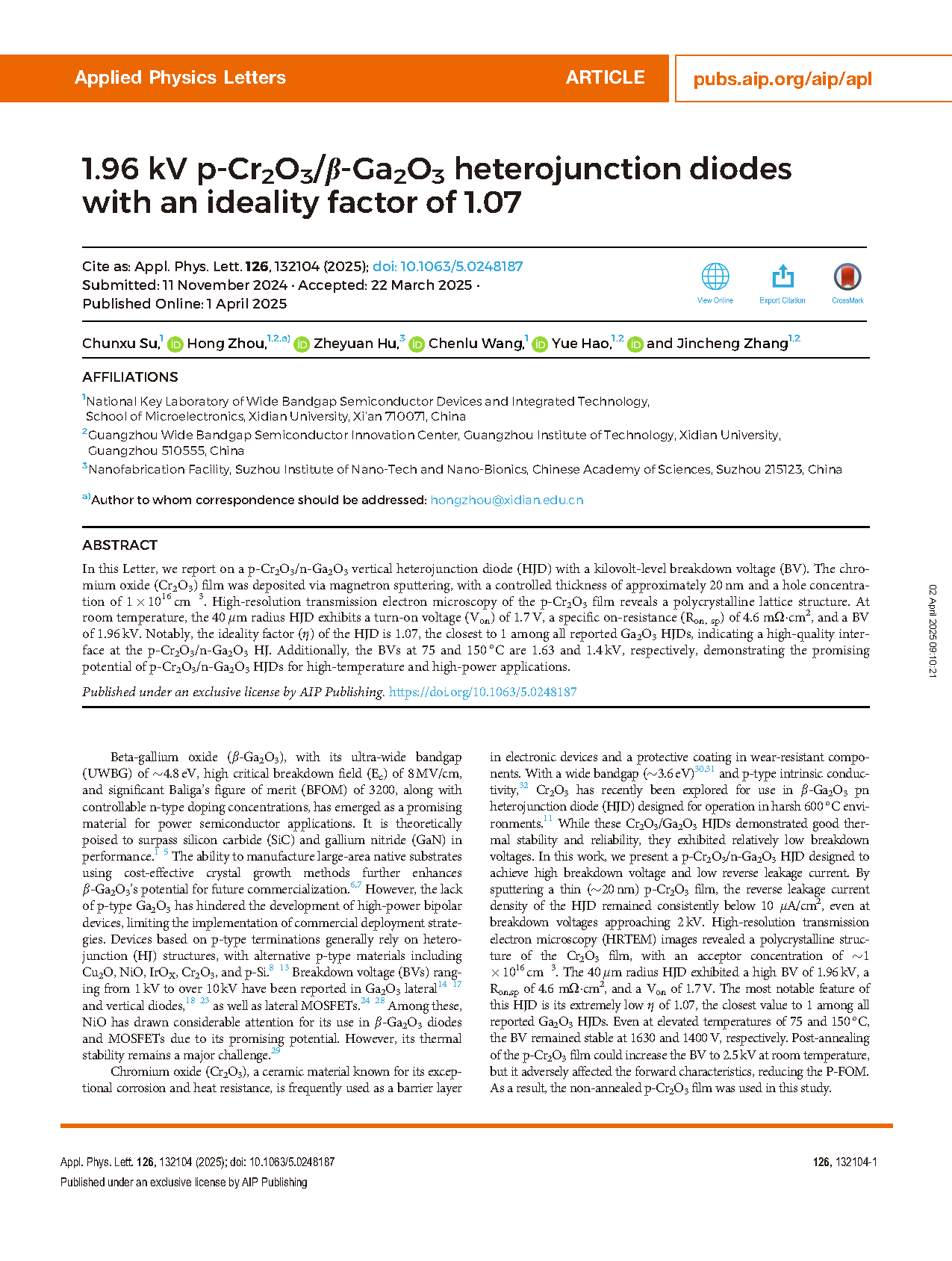
FIG. 1. (a) 2D cross-sectional schematic of the vertical p-Cr2O3/n- β-Ga2O3 HJD. (b) HRTEM images of HJD, and (c) HRTEM images of the Cr2O3/ Ga2O3 interface, and magnified inset on the right depicts the lattice structure image, reveals a polycrystalline structure of Cr2O3. (d) EDS elemental analysis results of the dashed box region in (b). (e) HRXRD 2θ-ω spectrum of 20 nm Cr2O3 film prepared on a sapphire substrate.
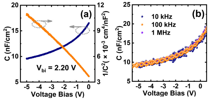
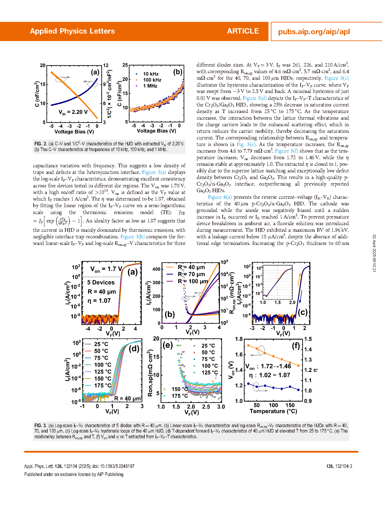
FIG. 2. (a) C–V and 1/C2 –V characteristics of the HJD with extracted Vbi of 2.20 V. (b) The C–V characteristics at frequencies of 10 kHz, 100 kHz, and 1 MHz.
DOI:
doi.org/10.1063/5.0248187