Paper Sharing
【Member Papers】Xidian University---Versatile optoelectronic memristor based on wide-bandgap Ga₂O₃ for artificial synapses and neuromorphic computing
日期:2025-04-17阅读:1138
Researchers from the Xidian University and Nanjing University have published a dissertation titled "Versatile optoelectronic memristor based on wide-bandgap Ga2O3 for artificial synapses and neuromorphic computing" in light: science & applications.
Acknowledgements
This work was financially supported by National Key Research and Development Program of China (Grant 2021YFA0715600, 2021YFA0717700, 2018YFB2202900), the National Natural Science Foundation of China (52192610, 62274127, 62374128, 62304167), 2023 Qinchuangyuan Construction Two Chain Integration Special Project (23LLRH0043), Key Research and Development Program of Shaanxi Province (Grant 2024GX-YBXM-512), CAS Project for Young Scientists in Basic Research (YSBR-113), the open fund of State Key Laboratory of Infrared Physics (SITP-NLIST-ZD-2023-03), the open research fund of Songshan Lake Materials Laboratory (2023SLABFN02), the Wuhu and Xidian University special fund for industry-university-research cooperation (XWYCXY-012021004), China Postdoctoral Science Foundation (2023TQ0255), the Fundamental Research Funds for the Central Universities and the Innovation Fund of Xidian University.
Background
The information technology industry has increased its demand for chip arithmetic power and energy efficiency due to the need to process large amounts of data quickly and effectively. The separation of data storage and computing components in the traditional von Neumann architecture gives rise to challenges such as “storage walls”, leading to substantial extra energy consumption and transmission delays. Consequently, scientists are creating innovative devices that mimic the human brain, allowing storage and processing in a single system. Neuromorphic computing, a type of computing, continues to drive the development of future computing systems. Resistive switching-based memristors, providing the benefits of low power consumption, multifaceted switching, fast switching speeds, and tiny cell sizes, are suitable for conventional complementary metal-oxide semiconductor (CMOS) technologies. Meanwhile, the storage and neuromorphic computation capabilities of the resistive switching-based memristors, make it the preferred option for non-volatile and neuromorphic computing applications. Up to now, neuromorphic computation has been implemented with a variety of materials, including organic semiconductors, perovskite, 2D materials, and oxide semiconductors. These materials provide a broad optical response spanning from the ultraviolet (UV) to near-infrared (NIR) region, restricting their applications in solar-blind detection.
Abstract
Optoelectronic memristors possess capabilities of data storage and mimicking human visual perception. They hold great promise in neuromorphic visual systems (NVs). This study introduces the amorphous wide-bandgap Ga2O3 photoelectric synaptic memristor, which achieves 3-bit data storage through the adjustment of current compliance (Icc) and the utilization of variable ultraviolet (UV-254 nm) light intensities. The “AND” and “OR” logic gates in memristor-aided logic (MAGIC) are implemented by utilizing voltage polarity and UV light as input signals. The device also exhibits highly stable synaptic characteristics such as paired-pulse facilitation (PPF), spike-intensity dependent plasticity (SIDP), spike-number dependent plasticity (SNDP), spike-time dependent plasticity (STDP), spike-frequency dependent plasticity (SFDP) and the learning experience behavior. Finally, when integrated into an artificial neural network (ANN), the Ag/Ga2O3/Pt memristive device mimicked optical pulse potentiation and electrical pulse depression with high pattern accuracy (90.7%). The single memristive cells with multifunctional features are promising candidates for optoelectronic memory storage, neuromorphic computing, and artificial visual perception applications.
Materials and methods
Device fabrication
The Ga2O3 thin film as an active switching layer was prepared by radio-frequency (RF) sputtering at 300 K. Throughout the sputtering process, the power and the air pressure were 120 W and 0.6 Pa, respectively. The flow rates of nitrogen and oxygen were adjusted to 45 sccm and 5 sccm, respectively. The thickness of the Ga2O3 thin film utilized in this device is 60 nm. The Ag electrodes are circular with a radius of 50 µm.
Characterization and measurements
Atomic force microscopy (AFM) was employed for surface morphology analysis. X-ray photoelectron spectroscopy (XPS, PHI VersaProbe 4) was performed to confirm the chemical composition of the Ga2O3 thin film. The crystalline structures of the Ga2O3 thin film were analyzed by an X-ray diffractometer (XRD, Bruker D8 Advance). The absorption spectra of the film were measured with a UV–vis spectrophotometer (Lambda950). The electronic and photoelectronic characteristics of the devices were investigated using a Keithley 4200-SCS semiconductor parameter analyzer under both dark conditions and 254/365 nm optical illumination. The ultraviolet light and pulses were generated by an LED controller (HPS-01A, CHIEF ELECTRO-OPTICS Instrument).
ANN simulation
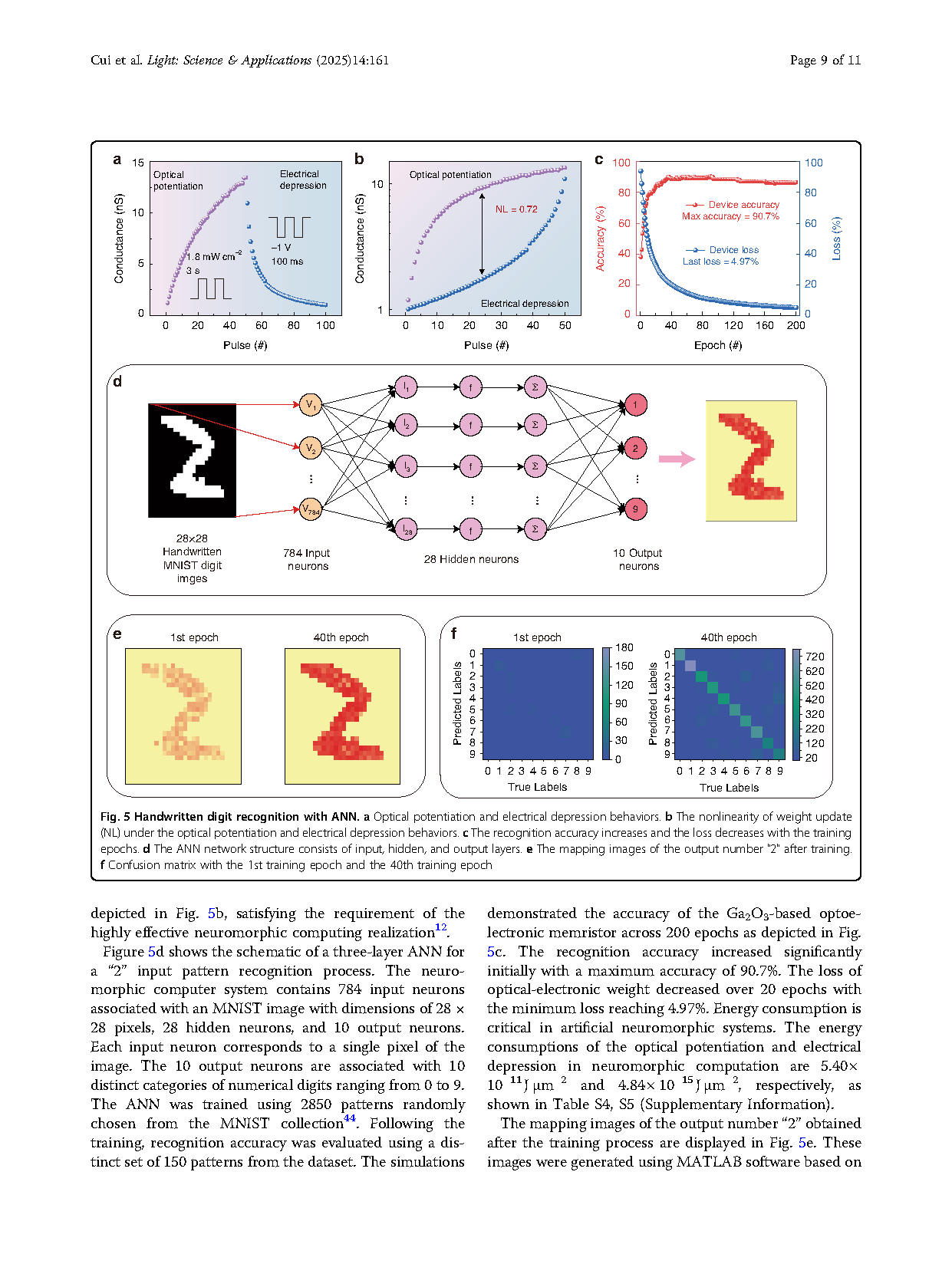
To investigate the optoelectronic-introduced synaptic behavior, we utilize a basic artificial neural network (ANN) for image recognition. Our work on neuromorphic vision systems is replicated using MATLAB. The training dataset is derived from the Modified National Institute of Standards and Technology (MNIST) database, a substantial collection of handwritten digits frequently employed to train diverse image processing systems. The training details for the ANN are shown in Table S6 (Supplementary Information).
Conclusion
The wide-bandgap Ga2O3-based optoelectrical synaptic memristor that integrates with data storage, optical synapses, logic gates, and neuromorphic computing is demonstrated. The MRS ability of the device is investigated by varying Icc and UV light intensities (254 nm). By altering the polarity of the input voltage, the memristor can perform the functions of two logic gates, AND and OR. The device has also demonstrated consistent synaptic characteristics such as PPF, SIDP, SNDP, STDP, and SFDP. When exposed to UV light, the device demonstrated advanced synaptic features such as LTM, STM, and learning-forgetting-relearning. In addition, the fabricated device could achieve a high pattern accuracy (90.7%) in ANN simulations. The integrated functions of optoelectronic memory storage and synaptic learning behavior make it a potential candidate for future in-memory computing systems.
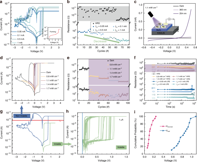
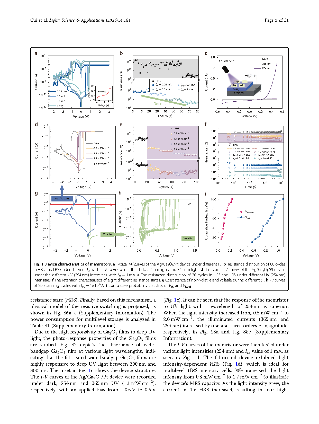
Fig. 1. Device characteristics of memristors. (a) Typical I-V curves of the Ag/Ga2O3/Pt device under different Icc. (b) Resistance distribution of 80 cycles in HRS and LRS under different Icc. (c) The I-V curves under the dark, 254 nm light, and 365 nm light. (d) The typical I-V curves of the Ag/Ga2O3/Pt device under the different UV (254 nm) intensities with Icc = 1 mA. (e) The resistance distribution of 20 cycles in HRS and LRS under different UV (254 nm) intensities. (f) The retention characteristics of eight different resistance states. (g) Coexistence of non-volatile and volatile during different Icc. (h) I-V curves of 20 scanning cycles with Icc = 1×10⁻⁶ A. (i) Cumulative probability statistics of Vth and Vhold
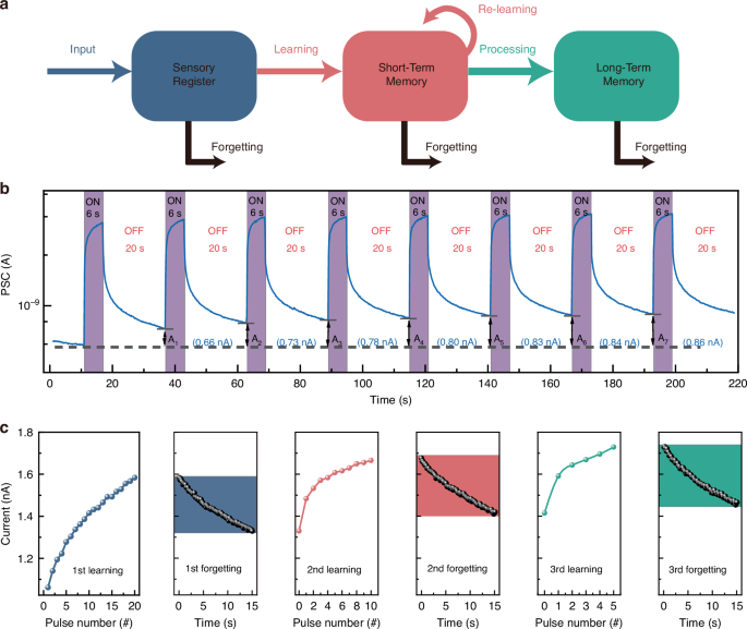
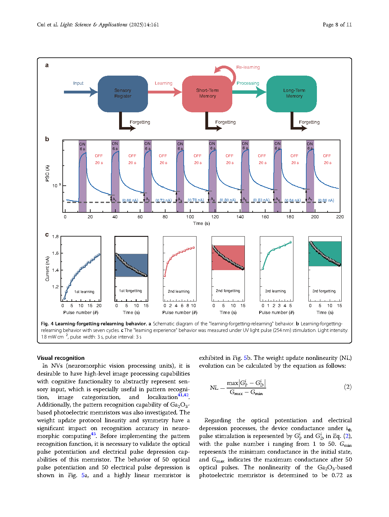
Fig. 2. Learning-forgetting-relearning behavior. (a) Schematic diagram of the “learning-forgetting-relearning” behavior. (b) Learning-forgetting-relearning behavior with seven cycles. (c) The “learning experience” behavior was measured under UV light pulse (254 nm) stimulation. Light intensity: 1.8 mW cm–2, pulse width: 3 s, pulse interval: 3 s
DOI:
doi.org/10.1038/s41377-025-01773-6