


News Trends
【Domestic News】Fourth-Generation Semiconductor Materials:Ushering in a Revolutionary Wave of Technological Innovation
日期:2025-04-18阅读:2332
Special Guide
Focus on Gallium Oxide
Diamond Exploring Performance Limits
Poised Potential of Aluminium Nitride
Semiconductor materials play a leading and foundational role in modern technological progress. Starting with Silicon (Si) and Germanium (Ge), moving on to Gallium Arsenide (GaAs) and Indium Phosphide (InP), and then to Silicon Carbide (SiC) and Gallium Nitride (GaN), these materials have been important drivers of the industry's development. At present, new semiconductor materials represented by Gallium Oxide (Ga₂O₃), Diamond (C) and Aluminum Nitride (AlN) are gradually becoming the focus, and many companies are accelerating their strategic layout. Innovative breakthroughs in single crystal growth technology, epitaxial thin films and other fields keep coming, and the construction of production lines and capacity expansion are also steadily advancing as planned.
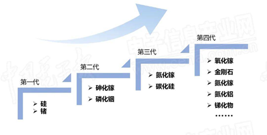
Advanced diagrams of representative semiconductor materials
1 Focus on Gallium Oxide
In the evolution diagram of semiconductor materials, Gallium Oxide, as a representative of the new generation of semiconductor materials, differs mainly from wide band gap semiconductor materials in its outstanding physical and chemical properties. Take the Bandgap as an example. The bandgap width of these new semiconductor materials exceeds 3.4 electron volts (eV), which is significantly higher than that of previous materials. This property enables them to function in a shorter wavelength range, especially showing great potential for applications in optoelectronic devices in the UVC region (200 nanometers to 280 nanometers). Gallium Oxide performs particularly well in this aspect.
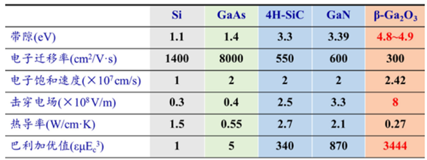
Comparison of various data of Gallium Oxide with other semiconductor materials
Gallium Oxide, as an emerging ultra-wide band gap semiconductor material, has a Bandgap of 4.9eV, significantly exceeding that of Silicon Carbide at 3.25eV and Gallium Nitride at 3.4eV. This characteristic enables Gallium Oxide to perform exceptionally well in terms of radiation resistance and high-temperature endurance, remaining stable in extreme temperature and radiation environments. In addition, the high breakdown field strength of Gallium Oxide ensures that its devices can operate under ultra-high voltage conditions, which helps to improve the carrier collection efficiency. Professor Li Chengming from the Institute of New Materials Technology at University of Science and Technology Beijing explained to China Electronics News.
These excellent properties of Gallium Oxide make it have great application prospects in the field of power devices. In the application of power devices, Gallium Oxide can withstand higher voltages, reduce energy loss, and thereby enhance power conversion efficiency. For instance, in the field of smart grids, Gallium Oxide devices can transmit and distribute electrical energy more efficiently, reducing the energy consumption of the grid. In new energy vehicle charging piles and inverters, Gallium Oxide devices are expected to enhance charging speed and vehicle energy utilization efficiency. Therefore, the industry generally holds a positive outlook on Gallium Oxide, believing that it is expected to replace Silicon Carbide and Gallium Nitride and become the representative of the new generation of automotive power semiconductor materials.
The market demand for Gallium Oxide is increasing day by day. Novell Crystal Technology (NCT), a Japanese enterprise, predicts that by 2030, the size of the Gallium Oxide wafer market will increase to approximately 59 billion yen. Fuji Keizai, a market research firm, also predicts that by then, the market size of Gallium Oxide power devices will reach 154.2 billion yen, exceeding the current market size of Gallium Nitride power devices.
Academician Hao Yue of the Chinese Academy of Sciences told China Electronics News in an interview that Gallium Oxide materials are expected to directly compete with Silicon Carbide and Gallium Nitride devices within the next decade, but the current research and development progress of Gallium Oxide still needs to be accelerated.
The slow progress in the research and development of Gallium Oxide chip technology is mainly attributed to the technical difficulties in its preparation process. The preparation methods of large-sized and low-defect Gallium Oxide single crystal and the ultra-precision processing technology of high surface quality Gallium Oxide wafer are the key bottlenecks. The high melting point of Gallium Oxide (approximately 1740℃) and its tendency to decompose and crack at high temperatures make the preparation of large-sized products extremely challenging. Traditional preparation processes, such as the EFG method, require a high temperature and oxygen-rich environment, which imposes very strict requirements on the growth environment. Iridium, as a precious metal suitable for holding Gallium Oxide melts, has a high cost that limits the expansion of the amount of equipment.
While research on iridium-free processes offers hope for cost reduction, these new processes are still in the early stages of exploration and are a long way off from industrial application. Optimizing these new processes, improving the stability of crystal growth quality, and reducing production costs are urgent issues that need to be addressed.
Researcher Yan Jianchang from the Institute of Semiconductors, Chinese Academy of Sciences, pointed out that the insufficient heat dissipation capacity of Gallium Oxide is its weakness. How to overcome this weakness and give full play to its advantages in power devices is the future development direction. Gallium Oxide still has great potential in device and industrial development. Its development foundation lies in the material itself and the preparation level. Achieving a lower defect density and fully tapping the material's advantages and potential are the keys to the development of ultra-wide band gap technology and industry.
The research and development road of Gallium Oxide is long and arduous. Since its establishment in 2015, NCT has been dedicated to the research and development of Gallium Oxide crystals. It was not until June 16, 2021, that it successfully mass-produced the world's first 100-millimeter Gallium Oxide wafer, laying the foundation for the wide application of Gallium Oxide in power semiconductors and other fields. At present, NCT holds a 90% share in the global Gallium Oxide single crystal substrate market and has achieved mass production of 6-inch Gallium Oxide wafers.
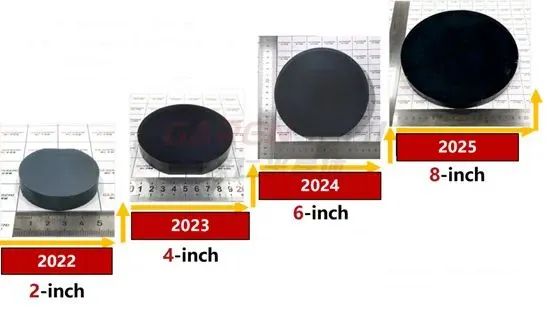
Evolution diagram of Gallium Oxide single crystal products of GAREN SEMI
China's progress in semiconductor material research and development has been accelerating and it has ranked among the world's leading. On March 5th, GAREN SEMI successfully launched the world's first 8-inch Gallium Oxide single crystal with its independently developed casting technology. This achievement marks China as the world's first country to master the 8-inch Gallium Oxide single crystal growth technology, breaking the long-standing competitive pattern of Gallium Oxide single crystal size dominated by Japan and followed closely by China, the United States and Europe. It is reported that the casting technology of Gallium oxide Semiconductor not only realizes the growth of 8-inch Gallium Oxide single crystal, but also can produce wafer substrates of corresponding sizes. Moreover, it is compatible with the existing 8-inch silicon-based chip production lines, effectively reducing production costs and improving production efficiency.
Meanwhile, Fuga Gallium announced a major breakthrough in Gallium Oxide MOCVD homogeneous epitaxy technology. For the first time, it has grown a homogeneous epitaxy film over 10 microns thick on a Gallium Oxide single crystal substrate. Its standardized products are scheduled to be officially launched on the market in April of the same year. In September 2024, Fuga Gallium Industry started the construction of China's first 6-inch Gallium Oxide single crystal and epitaxial wafer growth line in Fuyang, Hangzhou. It is expected to be put into use in early 2025 and will achieve an annual production capacity of 10,000 wafers in the future, further promoting the market supply and application of Gallium Oxide materials.
In addition to these two companies, there are also enterprises such as Beijing Gallium Family Technology, Suzhou GAO, and Suzhou Gayao Semiconductor in China, as well as some start-ups, that are engaged in the research and development of Gallium Oxide materials and devices, jointly promoting the rapid development of China in the field of new-generation semiconductor materials.
2 Diamond Exploring Performance Limits
Diamond, as a promising new generation of semiconductor material, has many remarkable physical properties. Professor Zhang Jinfeng from Xidian University pointed out in an interview with China Electronics News that diamond is a ultra-wide band gap semiconductor material, featuring wide band gap, high breakdown resistance, high carrier mobility, ultra-high thermal conductivity and strong radiation resistance. It has great application potential in fields such as heat sinks, high power, high-frequency devices, optical windows and quantum information.
Specifically, the bandgap of Diamond has reached 5.45eV, which is about three times that of Silicon. This makes Diamond have excellent stability and reliability in high-temperature and high-voltage environments. In addition, diamond has a thermal conductivity of up to 2200W/(m · K) at room temperature, which is 13 times that of Silicon, greatly enhancing the heat dissipation efficiency of the chip and thereby improving the performance and stability of electronic devices. Diamond also has a breakdown electric field strength of up to over 10MV/cm, which gives it a significant advantage in high-power, high-frequency device applications. These outstanding properties make diamond an ideal material for the semiconductor industry, capable of meeting future demands for high power, strong electric fields, and radiation resistance.
The experts believe that diamond semiconductors have broad application prospects in many fields. In the field of electronic information, Diamond-based high-frequency, high-power devices can be used in 5G and 6G communication base stations, significantly improving signal transmission speed and quality and reducing energy consumption. In the energy sector, Diamond-based power devices can be used in efficient energy conversion and storage systems, such as battery management systems for electric vehicles and photovoltaic inverters, to enhance energy utilization efficiency. In the aerospace field, the high stability and radiation resistance of Diamond semiconductors make them a key material for manufacturing high-performance radar, satellite communication equipment, etc. In addition, Diamond semiconductors also have broad application potential in medical, sensor and other fields.
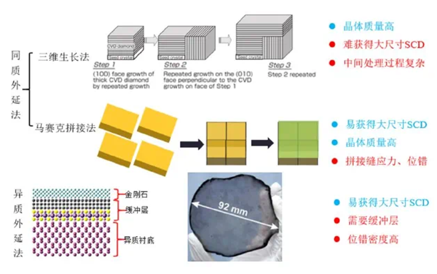
Schematic diagram of the growth route of large-sized single crystal Diamond
Despite this, the preparation technology of Diamond semiconductor materials still faces high difficulty and high cost, which limits the pace of its wide application, and there is an urgent need for breakthroughs in the preparation process. As the growth process of Diamond is extremely demanding in terms of equipment and technology, how to achieve efficient and low-cost production while ensuring the high quality of the material has become a top priority for the industry. In addition, the compatibility of Diamond with existing semiconductor processes is also an area that needs further exploration and improvement. Given the significant differences in physical and chemical properties between Diamond and traditional semiconductor materials, how to better integrate it into existing semiconductor manufacturing processes is crucial for the future applications of Diamond semiconductors.
Researchers began their studies on Diamond relatively early. As early as the 1970s, American researchers successfully grew small Diamond single crystal through the High-Temperature and High-Pressure method (HPHT), thus triggering a craze for diamond research.
According to Li Chengming's description, Diamond power electronics has made new technological advancements in both materials and devices. In terms of materials, the diameter of single crystal Diamond prepared by the High-Temperature and High-Pressure method has reached 20mm, and the defect density is relatively low. By using the Chemical Vapor Deposit (CVD) method, homogeneous epitaxial growth with low defect density can be achieved, and the size of independent single crystal wafers can reach 1 inch. By using the mosaic splicing technology of "tiled cloning" wafer, the size of diamond wafers can reach 2 inches. With heteroepitaxy technology, the wafers can reach 4 inches. Under the low-cost heteroepitaxy CVD method, the development and application of Diamond polycrystalline films are very active. The wafer size has reached 8 inches and can be used as a thermal conductive substrate for the next generation of GaN power electronic devices.
China has also made significant achievements in Diamond research. Yellow River Whirlwind, the world's leading producer of synthetic diamonds, has developed a polycrystalline Diamond heat sink with a thermal conductivity of over 2000W/m · K in collaboration with Huawei, thanks to its deep accumulation in HPHT and CVD technologies. This product is mainly used for heat dissipation in 5G base stations and AI chips, effectively solving the heat dissipation problem of high computing power equipment during operation. Huanghe Whirlwind is also actively laying out in the research and development of semiconductor substrate materials in an effort to secure a more favorable position in the Diamond semiconductor industry chain.
In the field of equipment, Beijing Sevenstar Electronics, a leading domestic semiconductor equipment enterprise, is actively engaged in the research and development of new generation semiconductor material equipment, providing crystal growth equipment for Diamond and other new generation semiconductor materials to many domestic research institutions. These crystal growth devices are key to the industrialization of semiconductor materials. They enable researchers to precisely control the growth conditions of Diamond crystals, produce high-quality Diamond substrates and epitaxial layers, and provide a solid foundation for the manufacturing of Diamond semiconductor devices.
3 Poised Potential of Aluminium Nitride
Aluminum Nitride, as an important component of ultra-wide band gap semiconductor materials, has a bandgap as high as 6.2eV, enabling it to function at shorter wavelengths and showing great potential especially in the field of deep ultraviolet optoelectronic devices. Aluminum Nitride also has a breakdown electric field strength of up to 15.4MV/cm, which enables it to withstand higher voltages and performs exceptionally well in high-power, high-voltage applications. In addition, Aluminum Nitride has an extremely high thermal conductivity of 340W/(m∙K), which gives it a significant advantage in heat dissipation, effectively addressing the overheating problem of the chip during high-power operation and enhancing the stability and reliability of electronic devices. Aluminum Nitride also has excellent chemical and thermal stability, as well as good UV transmittance.
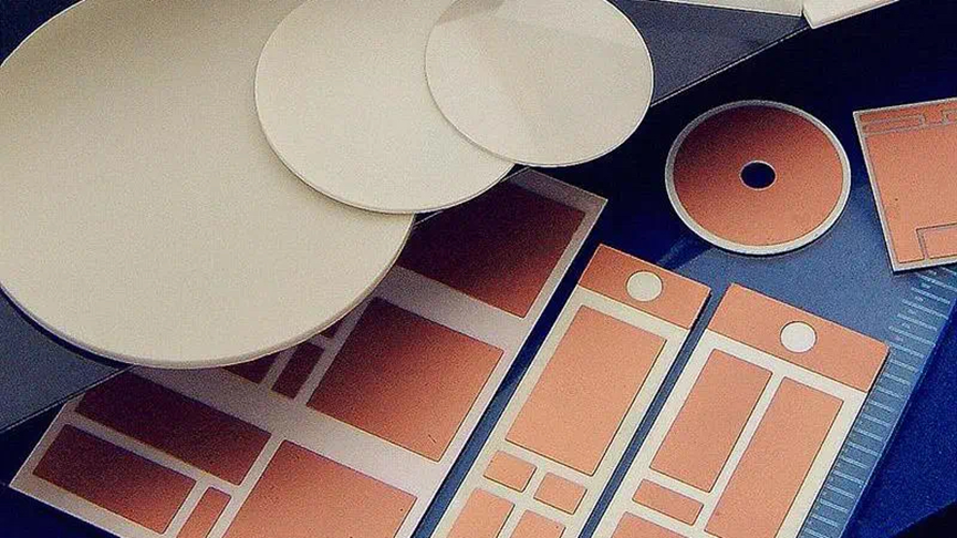
Aluminum Nitride ceramic substrate (Source: China Porcelain Electronics Official website)
Aluminum Nitride has a wide range of applications, especially in the power electronics industry. With the gradual electrification of various industries, the demand for efficient power conversion and distribution systems is on the rise. Devices made of Aluminum Nitride can effectively improve the energy conversion efficiency of these systems. Thanks to their ultra-wide bandgap, Aluminum Nitride devices can withstand voltages of more than 10 kilovolts, which not only helps to reduce the size of the system but also improves control performance. For instance, in grid-level applications, only a 15-micron-thick Aluminum Nitride substrate is needed to meet the requirements of a 10kV substation, with a volume reduction of 70% compared to traditional materials. According to a study by the Georgia Institute of Technology in the United States, Aluminum Nitride is seen as an ideal semiconductor material for the next generation of flexible smart grids. Another report shows that power devices based on Aluminum Nitride consume only one-eighth the energy of SiC/GaN devices during the DC-DC/DC-AC conversion process. In the 800V high-voltage platform of new energy vehicles, Aluminum Nitride can increase the efficiency of motor controllers by 5% and reduce the system loss of photovoltaic inverters by 30%.
In the microwave and radio frequency industry, in order to meet the demands of high-end applications such as 5G communication, satellite communication, and phased array radar, it is necessary to overcome the heat dissipation and high-temperature boundary issues of devices and modules. Aluminum Nitride-based devices can provide low thermal boundary resistance for commonly used Gallium Nitride RF high electron mobility transistors (GaN RF HEMTs) and have high bulk thermal conductivity, effectively solving the thermal management challenges of RF devices. Looking ahead, the power amplifier efficiency of 5G and even 6G base stations using aluminum nitride is expected to exceed 65%, energy consumption will be reduced by 40%, the power density of phase array radar can be increased by three times, and the detection range can be extended by 50%.
In the aerospace field, Aluminum Nitride material can ensure that deep earth probes operate stably for more than 100,000 hours in a geothermal environment of 300 ° C. In addition, Aluminum Nitride can enhance the radiation resistance of the space station's power system by 100 times and extend its lifetime to 15 years.
However, Aluminum Nitride still faces challenges in the preparation of large-sized and high-quality single crystal and in reducing dislocation density. On the one hand, the growth of Aluminum Nitride single crystal is rather difficult and the manufacturing cost is relatively high. On the other hand, the design and manufacturing process of Aluminum Nitride devices also need continuous innovation to fully leverage their performance advantages. Due to the differences in physical and chemical properties between Aluminum Nitride and traditional semiconductor materials, existing semiconductor manufacturing processes cannot be directly applied to the production of Aluminum Nitride devices, and there is an urgent need to develop new processes and equipment.
In terms of scientific research, significant progress has been made in Aluminum Nitride. The research team from the Fraunhofer-Institut für Integrierte Systeme und Bauelementetechnologie (Fraunhofer IISB) in Germany successfully prepared Aluminum Nitride epitaxial layers with low defect density by improving the crystal growth process. The Aluminum Nitride Schottky diode fabricated based on this epitaxial layer achieved a breakdown voltage of 2200 volts in the test and maintained a low on-resistance at high current densities. Its power density is significantly better than that of traditional Silicon Carbide and Gallium Nitride based power switching devices.
Crystal IS of the United States (a wholly-owned subsidiary of Asahi Kasei) has successfully developed 3-inch and 4-inch Aluminum Nitride single crystal substrate samples. China's Ultratrend Technologies Inc. has also achieved remarkable success in this field, successfully developing 3-inch Aluminum Nitride single crystal and 2-inch single crystal substrates with ultra-high deep ultraviolet light transmittance.
In addition to the above three major materials, there is also a new generation of semiconductors called ultra-narrow bandgap semiconductor materials, represented by Gallium Antimonide (GaSb) and Indium Antimonide (InSb), whose bandgap is within the range of a few tenths of an electron volt (eV). The electrons in these materials are prone to excitation transitions and have high mobility, and they are mainly used in infrared detection, lasers, and other fields. The application of Indium Antimonide in infrared detectors, with its high electron mobility and high sensitivity to infrared light, can quickly detect and precisely image weak infrared signals, and is widely used in industrial inspection, medical imaging and other fields; Gallium Antimonide plays an important role in the manufacturing of infrared lasers, which are suitable for scenarios such as optical communication and lidar, providing support for high-precision distance measurement and information transmission.
Overall, the new generation of semiconductor materials is of great significance to the development of the semiconductor industry. They are expected to break through the performance limitations of existing materials, meet the demands of future electronic devices for high performance, high reliability and low energy consumption, and drive the industry to a higher level. However, the research and development of the new generation of semiconductor materials are currently facing problems such as immature preparation processes, high costs, and poor compatibility with existing semiconductor manufacturing processes. In addition, as these materials are emerging fields, the industrial chain is not yet complete, and there are shortcomings in all links from raw material supply to equipment manufacturing and device packaging and testing. These factors have restricted the rapid development of the industry. Therefore, the industry should pay more attention to the research and development and industrialization of the next generation of semiconductor materials, promote collaborative innovation among all parties, and advance the industry.
