Conference News
【Conference News】Asian Gallium Oxide Alliance Invites You to the 3rd Jiufengshan Conference (JFSC) and Compound Semiconductor Industry Expo (CSE)
日期:2025-04-18阅读:2025
On April 23-25, 2025, the 3rd Jiufengshan Conference (JFSC) and Compound Semiconductor Industry Expo (CSE) will be held at Wuhan Optics Valley Science and Technology Exhibition Center. With the theme of "Activating the Future", the exhibition will conduct in-depth discussions on the cutting-edge technology, industry trend and future application of compound semiconductor.
Next, the alliance will take you to further understand the exhibitor distribution of the Compound Semiconductor Industry Expo and the introduction of the alliance member exhibitors.
Site Booth Map


Exhibitor of Alliance Member
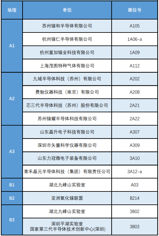
※ Exhibitors are listed in the order of venue zoning
AGOA with Members invite you to attend The 3rd Jiufengshan Conference (JFSC) and Compound Semiconductor Industry Expo (CSE)
Welcome to visit the booth for guidance!
Suzhou GAO Semiconductor Co., Ltd
Booth Number: A1-A105
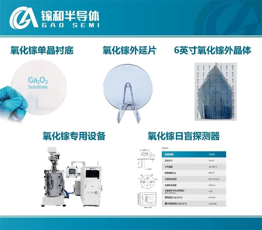
Suzhou GAO Semiconductor Co., Ltd is a high-tech enterprise focusing on the research and development of Gallium Oxide materials, and has always taken leading the technological innovation and application of Gallium Oxide as its mission. It is one of the few companies in China with comprehensive technology and capability of Gallium Oxide crystal growth, thin film epitaxy, related devices and special production equipment research and development.
Professor Tang Weihua, the founder of the company, has been deeply engaged in the field of Gallium Oxide materials for more than ten years. He took the lead in establishing and realizing the industrialization of Gallium Oxide in China, and established Suzhou GAO Semiconductor Co., Ltd in 2021. Since its establishment, the company has made a series of innovative achievements in the growth of Gallium Oxide crystals, and successfully achieved breakthroughs in large crystal size, high quality and multiple crystal face types, which has injected strong impetus into the development of the industry.
In the future, the company will take technological innovation as the core driving force, continue to explore the higher potential of Gallium Oxide materials, promote the deep integration of science and technology and industry, and strive to become a key force in building an efficient, green and intelligent future.
Hangzhou GAREN SEMI Co., LTD
Booth Number: A1-1A06-a
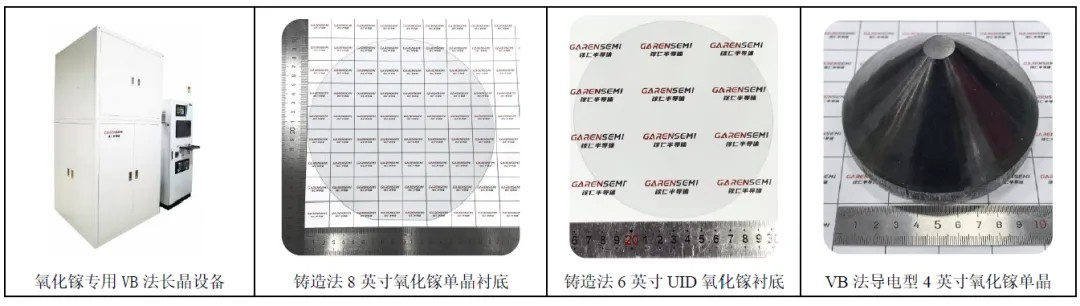
Hangzhou GAREN Semiconductor released the world's first 8-inch Gallium Oxide single crystal on March 5, 2025. GAREN SEMI is a technology enterprise focusing on the research and development, production and sales of wide band gap semiconductor materials such as Gallium Oxide. Relying on the National Key Laboratory of Silicon and Advanced Semiconductor Materials of Hangzhou International Science and Technology Innovation Center of Zhejiang University, the company has built a research and development, production and operation team with academicians of Chinese Academy of Sciences as the chief consultant and rich industry experience. The company created a new technology for Gallium Oxide single crystal growth, and obtained 14 international and domestic invention patents, breaking the monopoly and blockade of Western countries on Gallium Oxide substrate materials. Based on solving the major national needs, GAREN SEMI will be deeply engaged in the continuous innovation of the Gallium Oxide upstream industry chain, and strive to provide product guarantee for the development of China's power electronics and other industries.
GAREN SEMI leads the industry in innovation, achieving technological breakthroughs in the production of 6-inch Gallium Oxide single crystal substrates and wafer-grade (010) single crystal substrates using self-developed single crystal growth technologies such as the casting process, and developing the first dedicated Gallium Oxide VB long-crystal equipment including process packages. The company has mastered the core technology of Gallium Oxide growth, processing, epitaxy and other whole chain, providing customers with large-scale high-quality Gallium Oxide products and equipment with complete independent intellectual property rights.
Core Products
Hangzhou Fujia Gallium Technology Co., LTD
Booth Number : A1-1A09
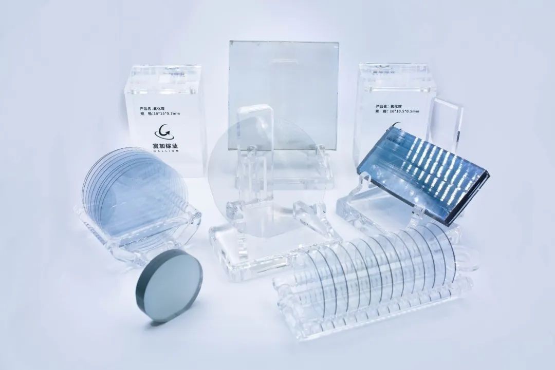
Hangzhou Fujia Gallium Technology Co., LTD., founded on December 31, 2019, is the first "hard technology" enterprise registered by Hangzhou Institute of Optics and Fine Mechanics. With the vision of "making the world use good materials", the company carries out the industrialization work of wide band gap semiconductor Gallium Oxide materials. The core products are Gallium Oxide single substrate, MOCVD epitaxial wafer, MBE epitaxial wafer, and Gallium Oxide crystal growth and processing equipment. The products mainly serve the fields of power devices, microwave radio frequency and photoelectric detection.
It has obtained 12 international patent licenses (6 in the United States and 6 in Japan), 40 domestic patent licenses, 3 trademark certification registrations of "Fujia Gallium" and 3 software Copyrights (" one-click crystal growth "control software).
Main Products
·2/4/6 inch Gallium Oxide wafer
·Gallium Oxide epitaxial wafer (MBE)
·Gallium Oxide epitaxial wafer (MOCVD)
·Gallium Oxide crystal growth furnace
·Gallium Oxide wafer polishing machine
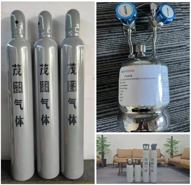
Shanghai Maotoo Specialty Gases Co.,Ltd
Booth Number: A1-A112

MAOTOOGAS, founded in 2008, specializes in the production and sales of gas products such as mixed gas, high purity gas, electronic gas, isotope gas, and gas pipeline supporting engineering services.
MAOTOO people pursue the spirit of forgetting themselves, without distractions, and continuous focus. Take this pursuit, MAOTOO GAS continued to serve the semiconductor, LED, optical fiber, the solar energy, petrochemical industry, biological medicine, military, scientific research in colleges and universities, electric power, electronics, shipbuilding, coal mining, automotive, medical, fire control, aerospace, food, building refining, fine chemical, processing and manufacturing industries.
MAOTOOGAS currently has production and R&D bases in Shanghai, Taicang, Jiangsu, Ezhou, Hubei, Quanjiao, Anhui and Quzhou, Zhejiang, serving customers all over the country. It has also set up companies in Hong Kong, Malaysia and North America, specializing in gas import and export business.
MAOTOOGAS is committed to becoming an excellent gas service provider. Guided by the values of integrity, practicality, diligence and responsibility, with the goal of creating self and pursuing no self, MAOTOO is committed to providing a development platform for employees, creating service value for customers, and contributing to the gas industry.
Main Products
Semianaly Semiconductor Technology(Suzhou)Co.,Ltd
Booth Number : A2-A202
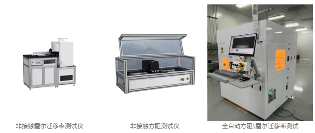
Founded in 2021, the company is a manufacturer of contactless semiconductor testing and analysis equipment with world-leading technology, registered in Suzhou. The company integrates research and development, design, manufacturing and sales, mainly overcoming foreign monopoly technology, replacing imported products, and making semiconductor material testing equipment domestic.
The main products: Non-contact nondestructive square resistance tester, wafer sheet resistance tester, sheet resistance tester, silicon resistivity tester, high and low resistivity analyzer eddy current method, bulk crystal resistivity analyzer, eddy current resistivity probe and PN probe tester, the migration rate (hall) tester, minority carrier lifetime tester, wafer and silicon wafer thickness tester, surface photovoltage JPV \ SPV. And provide testing and solutions for Silicon Carbide, silicon wafers, Gallium Nitride, Gallium Oxide, metal films, glass, substrates and epitaxy manufacturers.
With advanced technology and rich product lines, it has developed into one of the few semiconductor special equipment suppliers in Chinese Mainland with certain international competitiveness. Its products have been recognized by many mainstream semiconductor manufacturers at home and abroad, and have won good market reputation.
Main applications: Silicon Carbide testing, Gallium Nitride testing, wafer testing, Gallium Oxide testing, metal film testing, glass testing, substrate and epitaxial manufacturers, photovoltaic cell testing.
Main Products
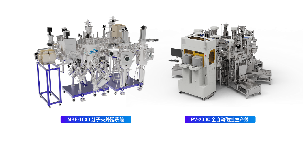
Fermion Instruments (Nanjing) Co., Ltd
Booth Number: A2-A208
Fermion Instruments (Nanjing) Co., Ltd, founded in 2017, is a national high-tech enterprise focusing on the development and manufacturing of high-end scientific research equipment. With the core values of "independence, innovation, persistence and integrity" and independent innovation, the company has made remarkable breakthroughs in the fields of molecular beam epitaxy (MBE) technology, ultra-high vacuum deposition coating technology and ultra-high vacuum magnetron sputtering technology, becoming one of the few manufacturers in China that can provide "one-stop total solution" for compound semiconductor epitaxy.
As an advanced MBE equipment manufacturer, Fermion Instruments has accumulated rich experience in ultra-high vacuum technology, precision machinery design, epitaxial process optimization and intelligent control system. The core products include large-size automatic molecular beam epitaxy equipment, ultra-high vacuum cleavage passivation system, and ultra-high vacuum automatic magnetic control production line, which can meet different needs from single 3inch process exploration to multi-piece 4inch mass production. Currently, Fermion Instruments equipment has entered the domestic semiconductor companies, research institutes and universities head, used in GaN power devices, antimonide type-II superlattice, ultra wide band gap semiconductor Ga2O3 materials, piezoelectric materials, high power laser and oxide technical indicators reached international advanced level.
Fermion Instruments will deeply cultivate the field of compound semiconductor equipment, promote technological progress through continuous innovation, and contribute the power of "China's intelligent manufacturing" to improve the autonomy level of semiconductor equipment in China. The company is committed to becoming an important participant in the global field of compound semiconductor epitaxial equipment, and working with the industry and academia to promote the innovation and development of semiconductor technology.
Si Century Semiconductor Technology(Suzhou)Co.,Ltd
Booth Number: A2-2A21
Founded in Suzhou Industrial Park in 2020, Si Century Semiconductor Technology(Suzhou)Co.,Ltd is a world-facing advanced semiconductor chip manufacturing equipment company with high-end talents and independent intellectual property rights, committed to building a world-leading key equipment and core technology platform for the semiconductor industry. The team's core management and technical experts have decades of successful experience in R&D and industrialization of a variety of high-end semiconductor chip manufacturing equipment.
At present, the company focuses on the research and development, manufacturing, sales and service of the third generation semiconductor epitaxy equipment such as SiC/GaN, providing domestic and foreign customers with chip manufacturing equipment and advanced technology solutions suitable for large-scale production and forward-looking scientific research, and will expand a variety of semiconductor equipment in the future.
Si Century Semiconductor is the first to achieve 6-inch and 8-inch vertical airflow silicon carbide epitaxy equipment mass sales manufacturers, equipment has entered more than a dozen industry head customers, and has carried out long-term mass production.
Technical Advantage
The equipment has completely independent intellectual property rights, with differentiated air intake mode, vertical airflow and temperature field control technology, supplemented by automatic loading and unloading (EFEM) system and high temperature disc and other means, to achieve the world's excellent low defect and other comprehensive technical indicators and performance. In high capacity, 8/6-inch compatibility, CoO cost, long-term multi-furnace continuous automatic growth control,
Low defect rate, ease of maintenance, reliability and other aspects have obvious advantages.
Suzhou Gayao Semiconductor Technology Co., Ltd
Booth Number: A2-2A22
Suzhou Gayao Semiconductor Technology Co., Ltd. is a high-tech enterprise specializing in CVD and ALD equipment manufacturing. The company is located in Kechuang Park, Zhangjiagang Free Trade Zone, Suzhou City, Jiangsu Province, covering an area of more than 1000 square meters. Since its establishment in 2022, the company has formed the product development department, process development department, product design department, equipment manufacturing department, quality department and other core departments, with a professional team of more than 20 people, including 15 technical personnel (more than 80% of bachelor degree or above).
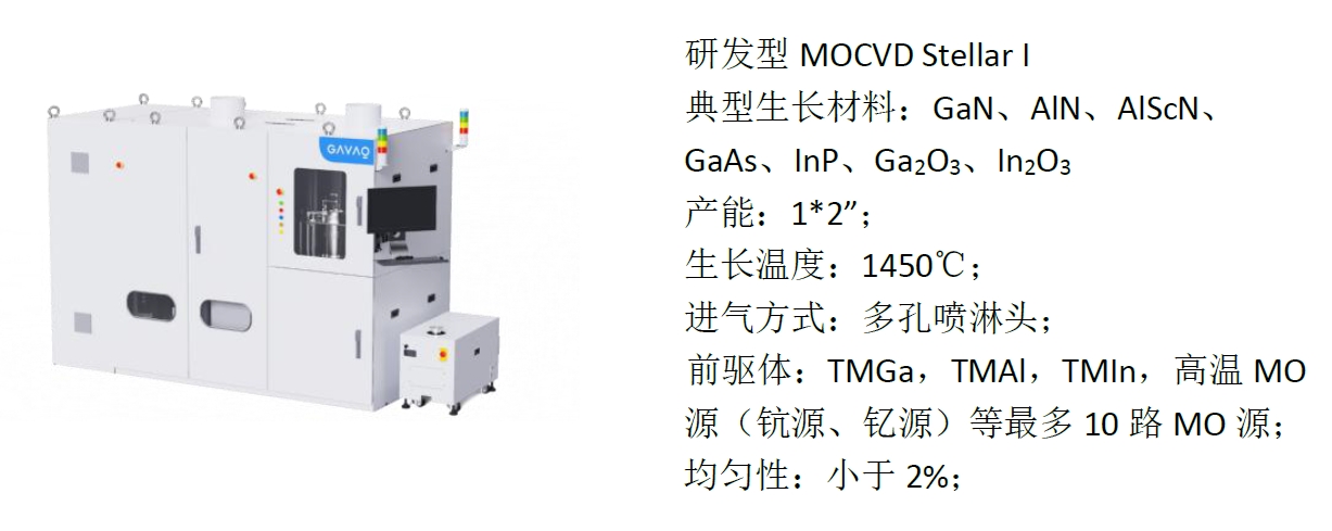
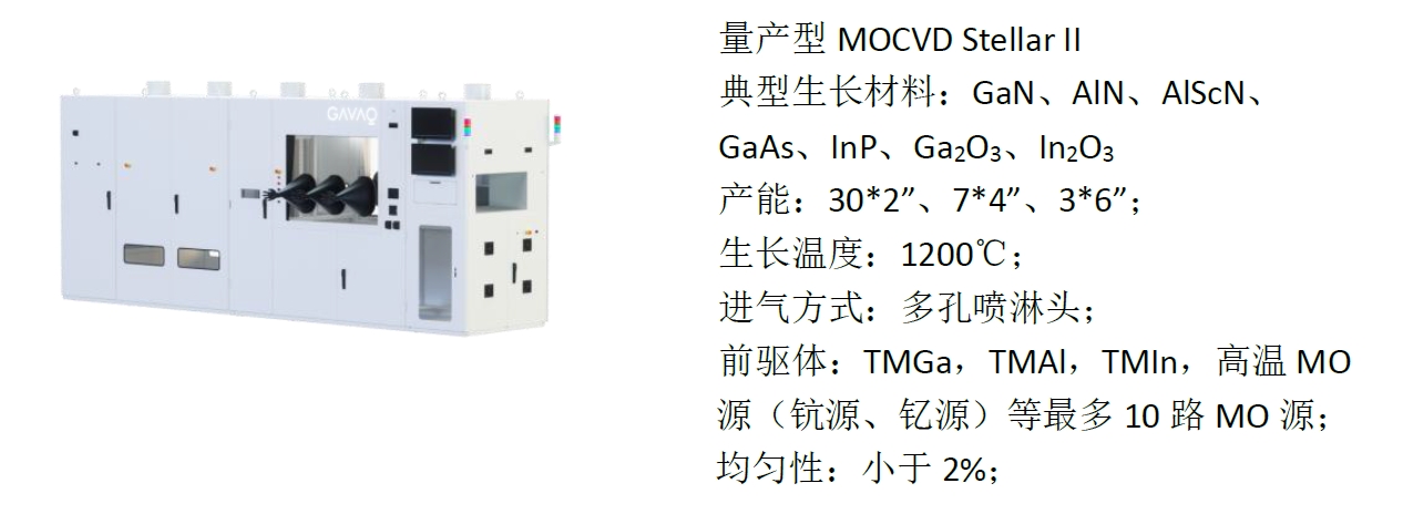
At present, the company's main products are Gallium Oxide MOCVD, Gallium Oxide MistCVD, Gallium Nitride MOCVD, Batch ALD equipment, monolithic ALD equipment, two-dimensional material CVD and a series of thin film deposition equipment. The products are mainly used for β phase - and E-phase Gallium Oxide epitaxy growth, α Gallium Oxide epitaxy growth. All kinds of oxide, nitride film deposition, MoS2 and other two-dimensional materials and Boron Nitride (BN) film growth, for the majority of scientific research institutions and enterprise users to provide a full range of film growth solutions.
Main Products
Shandong Jingsheng Electronic Technology Co., LTD
Booth number: A3-A307
Shandong Jingsheng Electronic Technology Co., Ltd. is a national-level high-tech enterprise focusing on the research and development and production of semiconductor equipment. The company's main products are the third and fourth generation semiconductor high-end equipment and a variety of crystal growth equipment, which are widely used in integrated circuit power devices, semiconductor materials, solar cells, LED chip manufacturing, new energy and other fields.
Jingsheng Electronics pays attention to technological innovation, owns a number of independent intellectual property rights, and is committed to providing customers with high quality products and solutions. Adhering to the business philosophy of "integrity, innovation, cooperation and win-win", the company continues to improve its core competitiveness and promote the technological progress of the industry.
Main Products
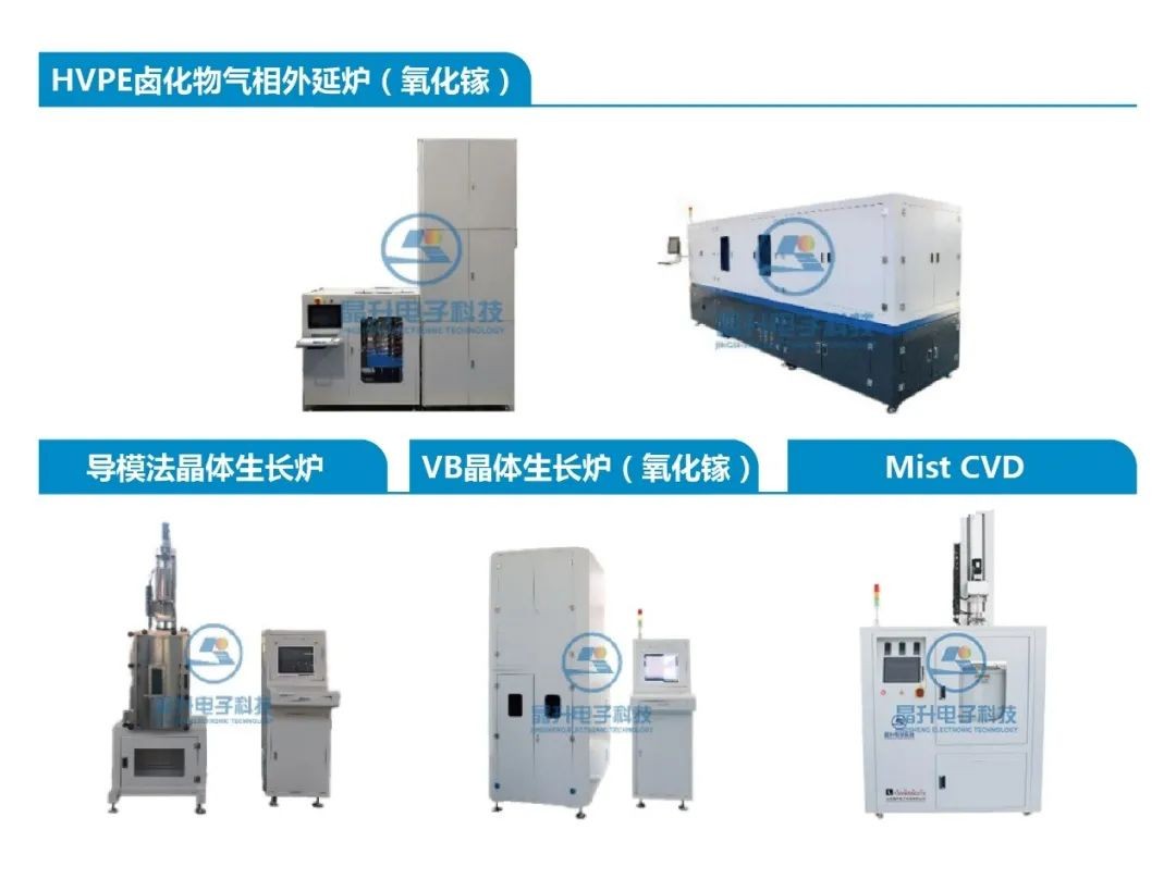
Silicon Carbide products: seed crystal bonding equipment, PVT crystal growth furnace, liquid phase crystal growth furnace, crystal annealing furnace, potassium hydroxide corrosion furnace.
Gallium Oxide products: VB crystal furnace, EFG method furnace, HVPE halide gas phase epitaxy furnace (Gallium Oxide), Mist CVD, etc.
Gallium Nitride products: HVPE crystal growth furnace, LPE Gallium Nitride high pressure crystal growth furnace.
Aluminum Nitride products: PVT crystal growth Furnace, LPE Aluminum Nitride high pressure crystal growth furnace.
Crystal lifting furnace, crucible drop crystal growth furnace, EFG furnace, etc.
Product Images
Shenzhen Vector Scientific Instrument Co., LTD
Booth Number: A3-A309
Shenzhen Vector Scientific Instrument Co., Ltd. was incubated in the team of Wuhan University, composed of many overseas returnees and domestic top schools, committed to pan-semiconductor experiment line, pilot line, production line equipment sales, process and factory technical services of national high-tech enterprises, innovative small and medium-sized enterprises, science and technology small and medium-sized enterprises, industrial enterprises above scale. It has authorized 32 patents and 14 software copyrights.
Main Products
① Lithography machine, PVD/CVD coating machine, etching machine, ion implantation machine, CMP, wet process equipment, oxidation annealing, advanced packaging equipment......
② Quantity detection and failure analysis equipment
③ Chip/device photoelectric test instrument
④ EPC engineering, factory engineering, secondary distribution engineering, factory operation and maintenance
⑤ "Vector laboratory" : 8-inch experimental line tape-out wafer foundry (8nm ~ μm), chip device testing services

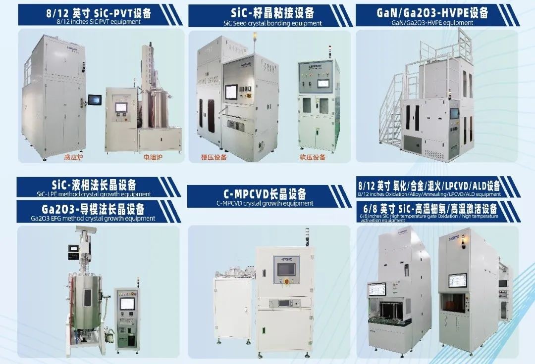
Shandong Liguan Microelectronics Equipment Co., LTD
Booth Number : A3-3A10
Shandong Liguan Microelectronics Equipment Co., LTD. (abbreviation: Shandong Liguan), founded in 2013. After 12 years of development, Shandong Liguan has become a domestic and foreign advanced semiconductor equipment manufacturing and process technology service provider integrating R&D, production and sales.
The company's products cover the first generation to the fourth generation of semiconductor material process equipment, all with independent intellectual property rights, completely independent and controllable, products are widely used in integrated circuits, power semiconductors, compound semiconductors, 5G chips, optical communication, MEMS and other new electronic device manufacturing fields.
The company can provide customers with an integrated solution of "equipment manufacturing + process technical service".
The company always firmly believes in the scientific development concept of "scientific and technological innovation is the first productive force", adheres to innovation-driven, innovation-led, and deeply cultivates the semiconductor industry. Committed to promoting the development of semiconductor material manufacturing and equipment technology, through continuous innovation and investment, constantly break through the technical bottleneck, improve product performance and quality, meet market demand, achieve localization substitution, promote the high-quality development of China's semiconductor industry, and contribute to the development of China's semiconductor industry.
Main products
I.Semiconductor process equipment:
1, Oxidation/diffusion/annealing equipment
Vertical furnace, horizontal furnace, SiC high temperature oxidation furnace, SiC high temperature annealing furnace
2, CVD equipment
LPCVD vertical furnace, LPCVD horizontal furnace
II. Compound crystal equipment:
1, SiC single crystal growth equipment
PVT furnace (induction furnace, resistance furnace), liquid phase crystal growth furnace, seed crystal bonding equipment (soft pressing equipment, hard pressing equipment)
2, GaN single crystal growth equipment
HVPE crystal growth furnace (horizontal, vertical)
3, Ga2O3 single crystal growth and epitaxy equipment
EFG crystal growth furnace, Vertical Bridgman method (VB) furnace (non-iridium technology), HVPE epitaxial furnace (horizontal, vertical)
4, diamond single crystal growth equipment
MPCVD crystal growth furnace
5, GaAs/InP single crystal growth equipment
Crucible lowering furnace
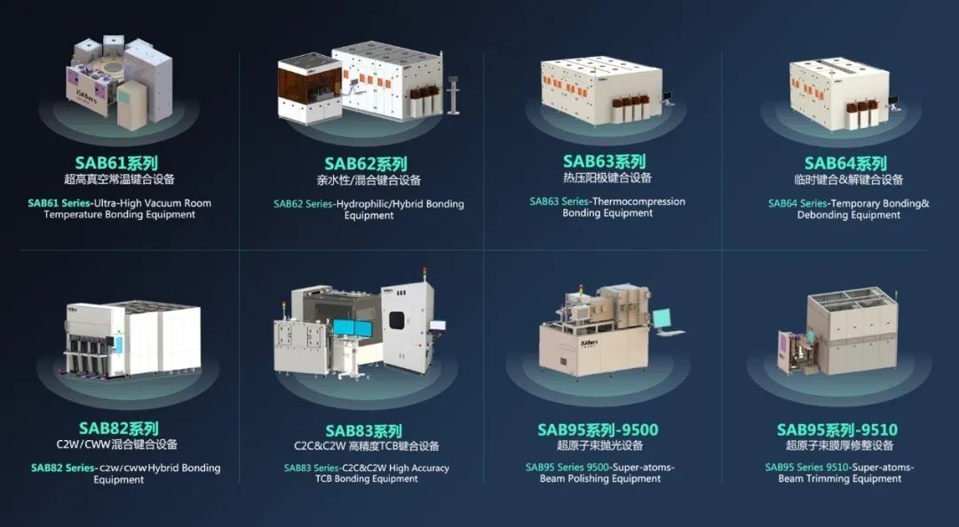
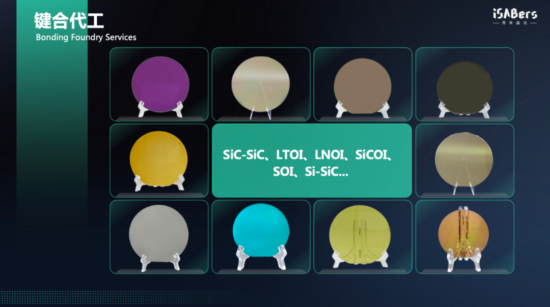
iSABers Group Co., Ltd.
Booth Number : A3-3A12-a
iSABers Group Co., Ltd. is a high-tech enterprise of semiconductor bonding integration technology in China. The company's core business covers high-end bonding equipment R & D and manufacturing and precision bonding process OEM, technology is widely used in advanced packaging, semiconductor device manufacturing, wafer-level heterogeneous material integration and MEMS sensors and other frontier fields, through the "equipment manufacturing + process service" two-wheel drive, to build the whole industry chain solution, has successfully developed four independent intellectual property product matrix: Ultra high vacuum room temperature bonding system, hybrid bonding equipment, hot pressing bonding equipment and supporting process services. Through continuous technological innovation, the company is committed to providing high-precision, stable process and cost-effective bonding equipment and solutions for the global semiconductor industry chain, and support the rise of strategic emerging industries.
Core Technology
1, Surface activation bonding: master a full set of surface activation technology such as ICP\CCP\FAB, which can cover a whole series of bonding equipment scenarios;
2, Sub-micron precision alignment technology: master the mainstream sub-micron alignment technology such as Face to Face, interchip coaxial, infrared penetration;
3, Ultra-high vacuum technology: in the ultra-high vacuum environment to complete activation, alignment and other processes, break through the challenges brought by vacuum;
4, Temperature control and pressure bonding technology: to ensure high temperature, high pressure Homogeneity;
5, Single rotary coating/cleaning technology: high-speed rotating dynamic balance, to prevent backsplash pollution, to ensure high bonding yield.
High-End Bonding Equipment Series
Craft OEM Series
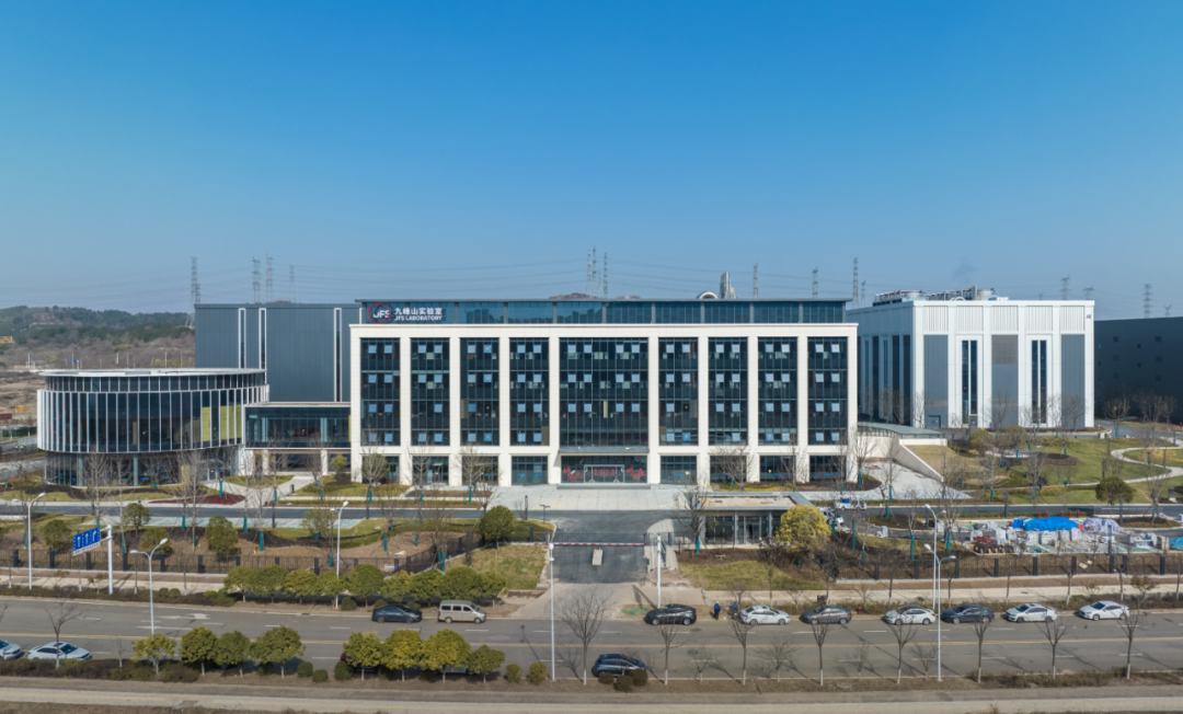
Hubei Jiufengshan Laboratory
Booth Number: B1-A03/B3-3B02
With the vision of building the world's leading compound semiconductor R&D and innovation center, Jiufengshan Laboratory brings together talents from all over the world to create an open, public and shared research platform to build a sustainable future with partners. Since its establishment four years ago, Jiufengshan Laboratory has established an advanced compound semiconductor research and pilot test platform in Optics Valley, China, with a number of international and domestic pioneering achievements. In the future, Jiufengshan Laboratory will adhere to the use-oriented approach, work with partners to promote scientific progress and the development of compound semiconductor industry, and accelerate the building of a global compound semiconductor platform, technology and industry "lighthouse".
Asian Gallium Oxide Alliance
Booth Number : B2-B214
Founded in July 2022, the Asian Gallium Oxide Alliance (AGOA) is a professional organization jointly initiated by a number of top universities, research institutions and industry units in Asia to promote innovation and development of ultra-wide band gap semiconductor new materials industry. The Asian Gallium Oxide Alliance officially registered and established the operating unit "Hangzhou Fuyang Gallium Valley Gallium Oxide Industry Development Service Center" in January 2024. The organization is a private non enterprise unit. By the end of 2024, the alliance has successfully absorbed nearly 60 member units, covering the upstream and downstream resources of the Gallium Oxide industry chain, forming a strong collaborative innovation network.
By the end of 2024, the alliance has successfully absorbed nearly 60 member units, covering the upstream and downstream resources of the Gallium Oxide industry chain, forming a strong collaborative innovation network.
Shenzhen Pinghu Laboratory
National Center of Technology Innovation for Wide Bandgap Semiconductor (Shenzhen)
Booth Number: B3-3B03
National Center of Technology Innovation for Wide Bandgap Semiconductor (Shenzhen) was awarded by the Ministry of Science and Technology in December 2021 and held by Shenzhen Municipal Science, Technology and Innovation Commission in August 2022. Shenzhen Pinghu Laboratory was established as the main operating unit, focusing on SiC and GaN and the next generation of advanced power electronic materials and devices, core equipment and parts, supporting materials and other fields. To carry out core technology research.
The laboratory is located in Luoshan Science and Technology Park, Longgang District, Shenzhen, covering an area of 130 mu, 100 class clean room area of 9500 square meters, with industry-leading wide band gap power semiconductor infrastructure, more than 380 sets of international and domestic advanced equipment. The laboratory has a manpower of over 390 people, bringing together top talents at domestic and international to build an open, public and shared scientific research, pilot test and analysis platform for the whole country, and jointly build a sustainable future.