Paper Sharing
【Domestic Papers】High-performance Sn-doped Ga₂O₃ FETs by co-sputtering: Depletion mode versus enhancement mode
日期:2025-04-21阅读:851
Researchers from the Beijing Institute of Technology have published a dissertation titled "High-performance Sn-doped Ga2O3 FETs by co-sputtering: Depletion mode versus enhancement mode" in Materials Science in Semiconductor Processing.
Project Support
This work was supported by the National Key R&D Program of China(No.2023YFB3611700) and National Natural Science Foundation of China(92163206, 12321004).
Background
As an ultrawide-bandgap semiconductor, gallium oxide (Ga2O3) typically presents a bandgap larger than 4.5 eV and a high critical breakdown field of 8 MV/cm. Besides, the Baliga figure of merit (BFOM) of Ga2O3 can theoretically exceed 3000, which is significantly larger than those of GaN (∼870) and SiC (∼340). Recently, Ga2O3 has been extensively explored for field-effect transistors (FETs), the current capability of which can be effectively improved with Sn, Ge, and Si doping. Specifically, Sn dopants in Ga2O3, existing as Sn4+ to substitute Ga3+, elevate electron concentration, enabling a conversion from insulator-like pristine Ga2O3 to semiconductor. This conversion can notably boost the on-state current (ION) of the Ga2O3 FETs more than 107 times. However, FETs with doped Ga2O3 are always in depletion-mode (d-mode) operation but the enhancement-mode (e-mode) devices are desirable because the normally-off operation is safe and energy-saving for power applications. One method to fabricate e-mode doped-Ga2O3 FETs is to intentionally reduce the channel carrier density, which can simultaneously decrease the ION. Another method is to adopt novel device architectures like fin-shaped channels and vertical transistors, which can complicate fabrication processes and raise production costs. Moreover, high temperature and homogeneous substrates are always required in the preparation of Ga2O3, limiting the handy modulation of operation modes and mass production feasibility.
Abstract
High-performance Sn-doped gallium oxide (Ga2O3) films were deposited on Si/SiO2 substrates to fabricate field-effect transistors (FETs) via room-temperature co-sputtering. The performances of the SiO2-supported FETs were optimized by varying the co-sputtering power of Sn to demonstrate a large on-state current (ION) of 2.5 mA/mm and a high on/off ratio of over 106. However, it is accompanied by a normally-on behavior with a negative threshold voltage (VTH), namely depletion mode (d-mode). Importantly, this d-mode can be converted to enhancement mode (e-mode) by adopting high-k Ta2O5/pristine Ga2O3 dielectrics, and extra nitrogen (N) doping in the Sn-doped Ga2O3 channels. Finally, the performances of the e-mode FETs with high-k dielectrics can be promoted via a Sn-doped Ga2O3/(Sn, N)-doped Ga2O3 dual-layer channel structure, which presents a large ION over 2 mA/mm, a high on/off ratio exceeding 107, and a small VTH below 5 V. Furthermore, the FET with dual-layer channel shows excellent stability, which is reflected by the bias stress measurement and stable performances after 3-month exposure to air. This remarkably-improved performance is attributed to the enhanced field effect by the high-k dielectrics, and the dual-layer channel structure that possesses both high stability of the (Sn, N)-doped layer and high current capability of the Sn-doped layer.
Highlights
• High-performance Sn-doped Ga2O3FETs are fabricated via co-sputtering method.
• The conversion from depletion mode to enhancement mode is successfully achieved.
• Excellent stability is obtained by developing a dual-layer channel of (Sn, N)-doped Ga2O3/Sn-doped Ga2O3.
Conclusions
In this work, e-mode Sn-doped Ga2O3 FETs with high-k Ta2O5 gate dielectrics were fabricated by co-sputtering at room temperature. Based on the high-k Ta2O5, other methods of pristine Ga2O3 buffer layer for Ta2O5, nitrogen doping, and dual-layer channel are further explored, which significantly reduce the IOFF and positively shift the VTH to achieve the e-mode operation. Moreover, the device with dual-layer channel exhibits excellent stability for long-term storage and bias-stress measurement. Finally, averaged over 20 devices, the dual-channel FETs with high-k Ta2O5/pristine Ga2O3 dielectrics show a high ION over 2 mA/mm, a large ION/IOFF over 2 × 10⁷, and a small positive VTH below 5 V. Therefore, this study provides an efficient and low-cost method for the wafer-scale fabrication of Si-compatible Ga2O3 nanodevices to enable low-temperature processing and facilitates heterogeneous power integration. Moreover, the high performances in this work can also highlight the versatility and potential of these devices for a wide range of electronic devices.
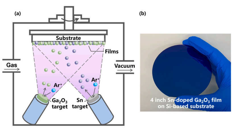
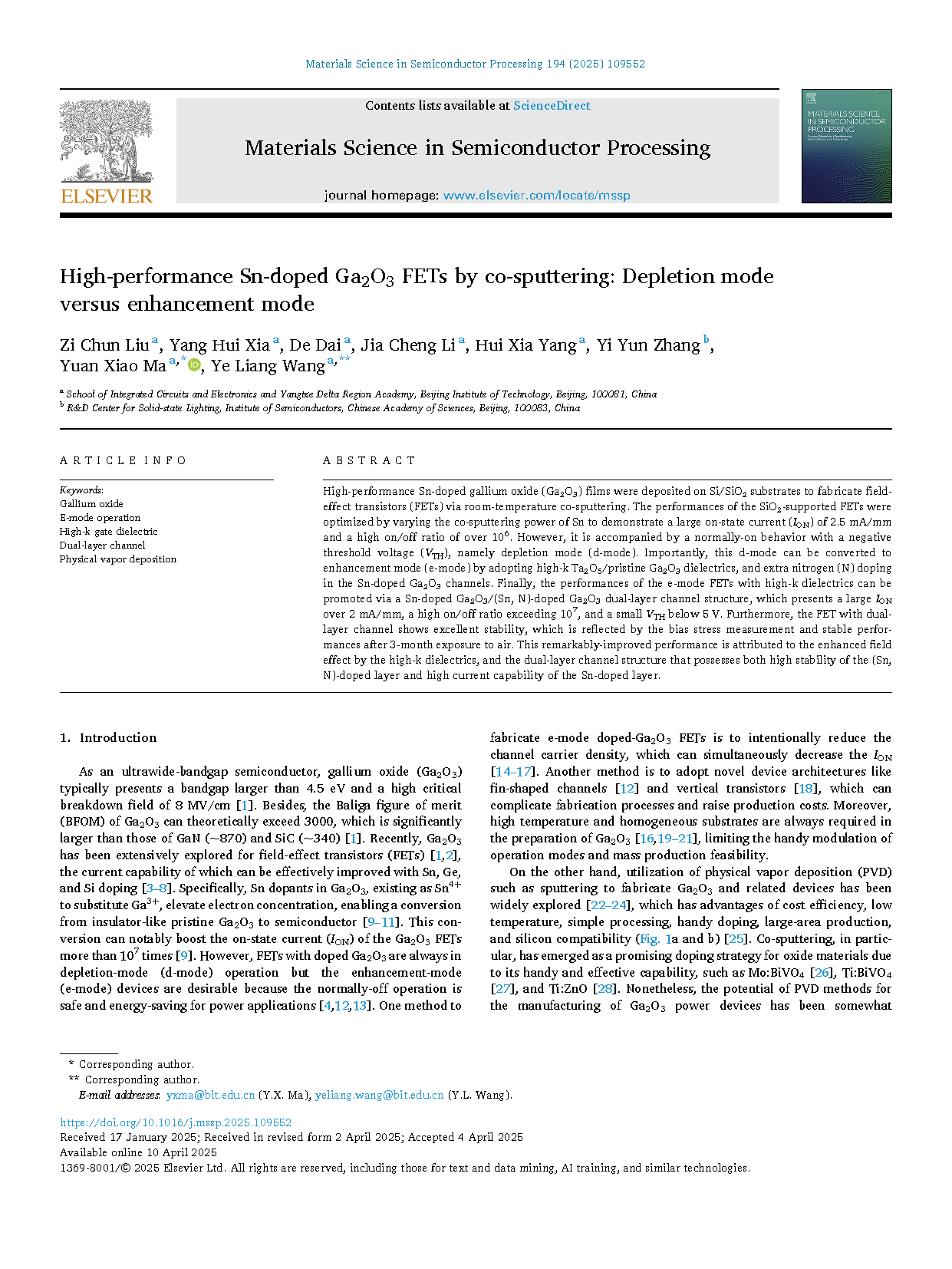
Fig. 1. (a) Schematic diagram of the preparation of Sn-doped Ga2O3 films via co-sputtering method. (b) The handy wafer-scale preparation of Sn-doped Ga2O3 film on a 4 inch Si/SiO2 wafer.
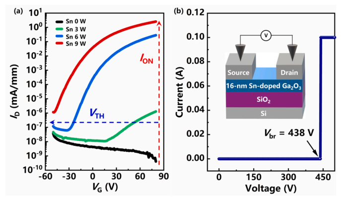
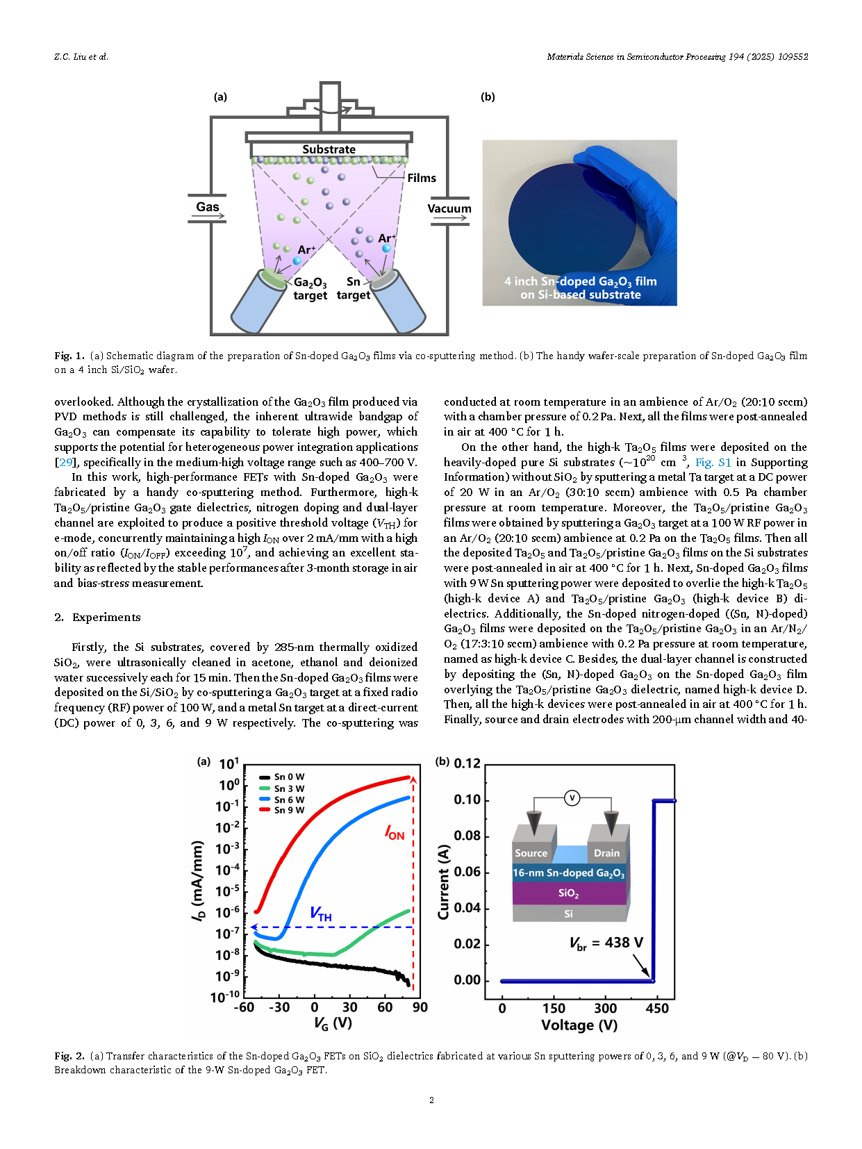
Fig. 2. (a) Transfer characteristics of the Sn-doped Ga2O3 FETs on SiO2 dielectrics fabricated at various Sn sputtering powers of 0, 3, 6, and 9 W (@VD = 80 V). (b) Breakdown characteristic of the 9-W Sn-doped Ga2O3 FET.
DOI:
doi.org/10.1016/j.mssp.2025.109552