Paper Sharing
【International Papers】p-CuGaO₂/β-Ga₂O₃ interfaces: A high-throughput approach for interface prediction and generation for power device applications
日期:2025-05-08阅读:886
Researchers from the Sejong University have published a dissertation titled "p-CuGaO2/β-Ga2O3 interfaces: A high-throughput approach for interface prediction and generation for power device applications" in Materials Today Advances.
Abstract
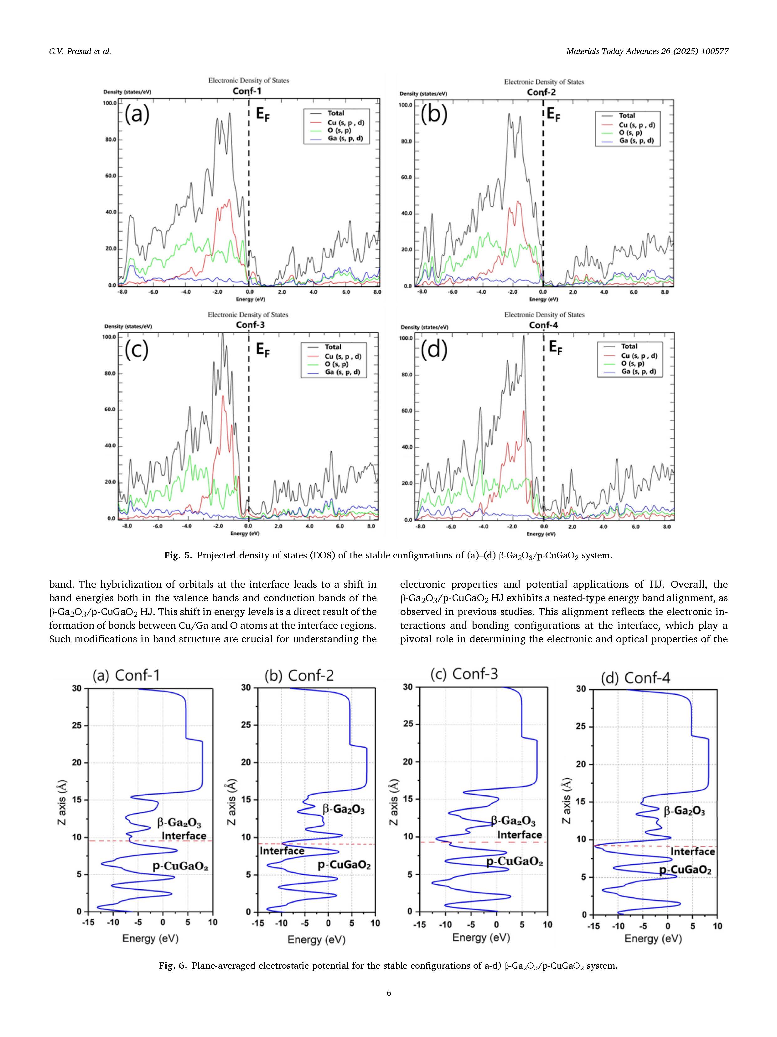
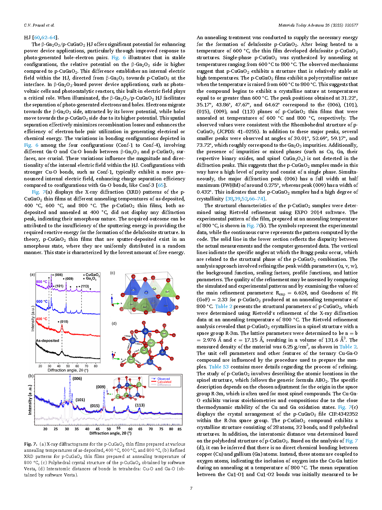
This study integrates a p-type copper gallium oxide (p-CuGaO2) interlayer to enhance the performance of β-Ga2O3-based power devices, addressing challenges in achieving reliable p-type doping. The p-CuGaO2 interlayer is expected to improve breakdown voltage (BV) and reduce leakage current, increasing device efficiency and reliability under high-temperature conditions. The heterojunction (HJ) system of β-Ga2O3 and p-CuGaO2 is investigated using density functional theory (DFT) via the Vienna Ab initio Simulation Package (VASP) and experimental methods, focusing on the β-Ga2O3 (001)/p-CuGaO2 (006) interface. Binding energy, electron localization, charge density difference, and electrostatic potential drop are analyzed, identifying Configuration-1 as the optimal configuration due to its high binding energy and favorable structural properties. Annealing temperature impacts the microstructure, stoichiometry, optical, electrical, and transport properties of p-CuGaO2/β-Ga2O3 HJs. Electrical measurements reveal reduced turn-on voltage (Von), on-resistance (Ron), and leakage currents, with the highest BV of 1.62 kV achieved at 800 °C compared to Pt/β-Ga2O3 Schottky barrier diode (SBD). The interface state density (NSS) is evaluated using the high-low frequency approach. Silvaco TCAD simulations explore breakdown mechanisms, demonstrating the potential of p-CuGaO2 for β-Ga2O3 HJ power devices. These findings support the development and manufacture of robust β-Ga2O3 HJ power devices.
Highlights
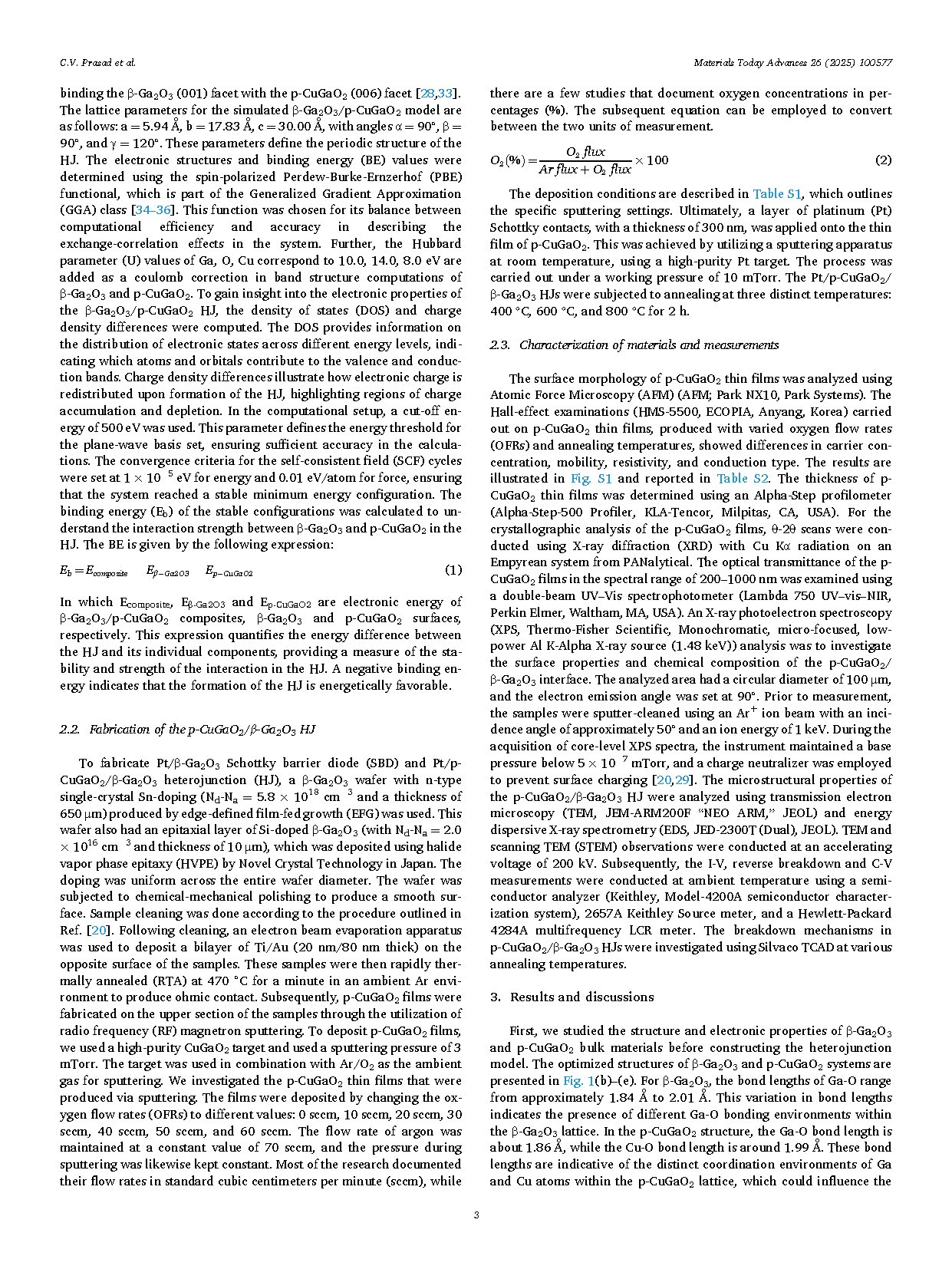
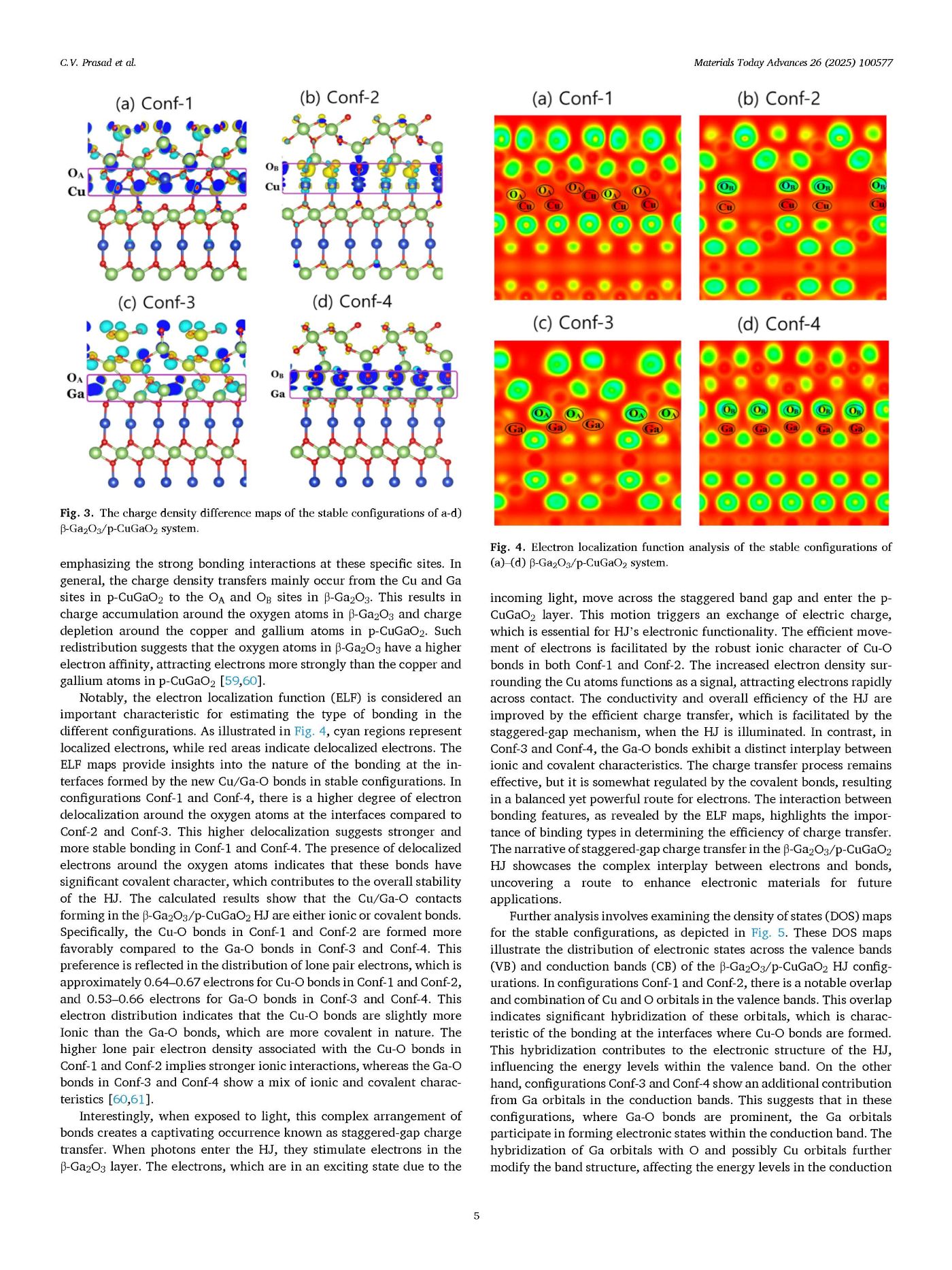
The p-CuGaO2(006)/β-Ga2O3 (001) interface models with four heterostructures were investigated using the first principles based on DFT studies.
The p-CuGaO2/β-Ga2O3HJ annealed at 800 °C exhibits superior electrical characteristics including as compared to the as-deposited, 400 °C-annealed, and 600 °C-annealed samples.
The p-CuGaO2/β-Ga2O3HJs demonstrated their potential for high-temperature operation by achieving the highest BV of 1.62 kV at 800 °C.
Silvaco TCAD simulations explore breakdown mechanisms, demonstrating the potential of p-CuGaO2/β-Ga2O3HJ power devices.
The annealing process at 800 °C resulted in p-CuGaO2/β-Ga2O3HJs with excellent electrical properties and high quality, demonstrating their considerable potential for high-temperature applications.
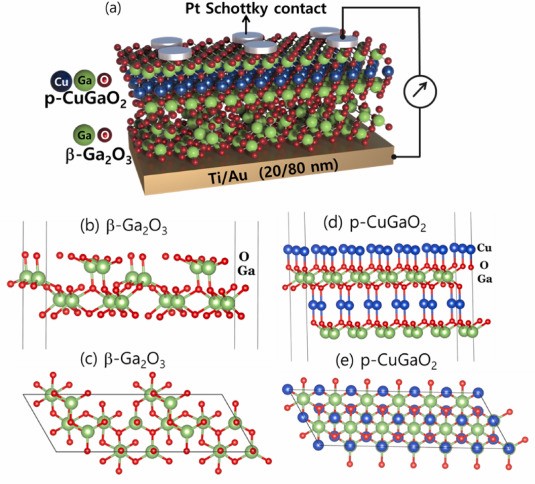
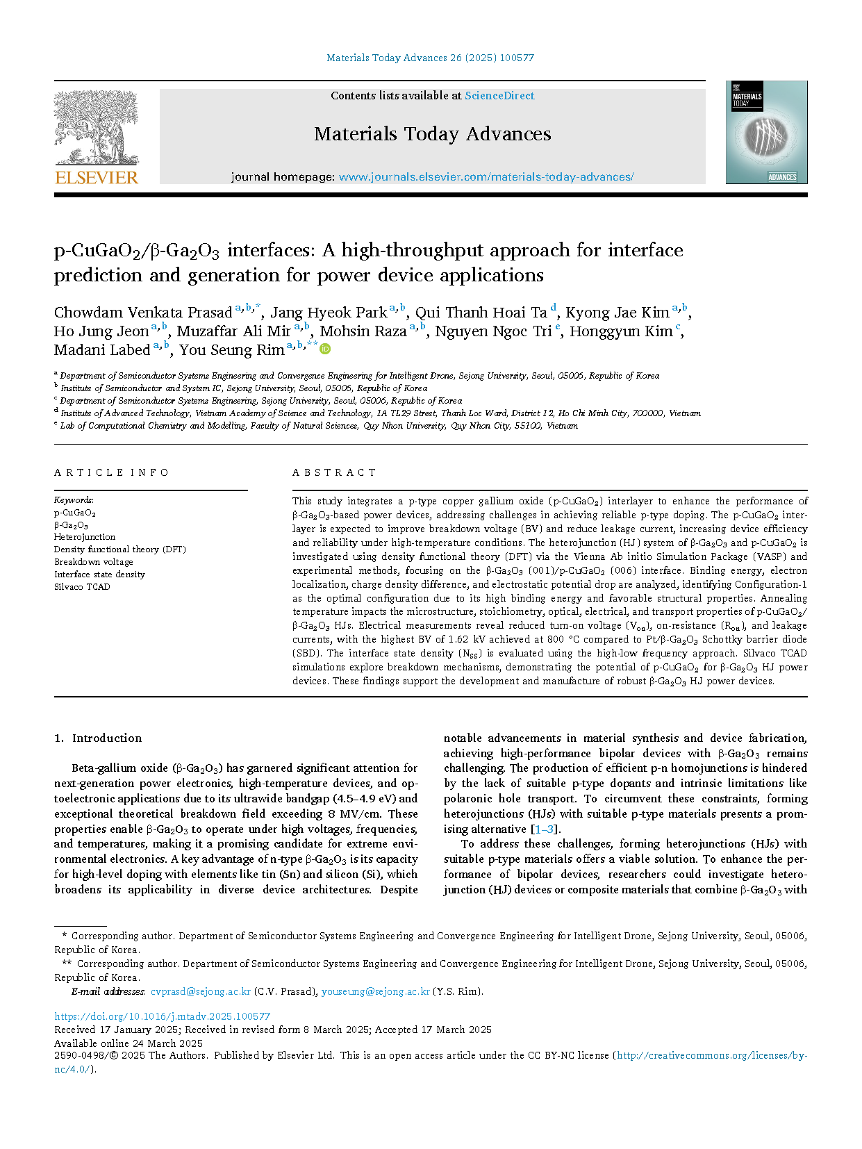
Fig. 1. (a) Illustrates the design of the vertical Pt/p-CuGaO2/β-Ga2O3 HJ, and the surface models (front and top views) of (b)–(c) β-Ga2O3, (d)–(e) p-CuGaO2 (Ga, O, and Cu atoms are displayed in green, red, and blue colors, respectively).
Fig. 2. The optimized configurations of (a-d) β-Ga2O3/p-CuGaO2 system.
DOI:
doi.org/10.1016/j.mtadv.2025.100577