


News Trends
【Domestic News】Will Gallium Oxide Change the World in Near Future?
日期:2023-03-14阅读:1251
We have all been brainwashed by the saying "Charge for 5 minutes, Talk for 2 hours". Who could refuse a fast but compact charging plug?
Since mobile phone manufacturers used gallium nitride (GaN) in fast charging, this third-generation semiconductor material has almost become the standard for fast charging.
When you are using the charging plug made of gallium nitride, scientists and industry have already targeted the stronger fourth generation semiconductor material: gallium oxide (Ga2O3), which can make a more powerful charging plug.
At present, more than two thirds of domestic semiconductor products are completely dependent on imports, and high-end semiconductor materials are even more scarce. But gallium oxide is different. This new material is on the eve of industrialization at home and abroad. We have the potential to make breakthroughs and surpass, so it is worth paying close attention to.
At the peak at birth
There are many "potential advantages" in the fourth generation of semiconductor materials, though aluminum nitride (AlN) and diamond still face a large number of scientific problems unsolved. Gallium oxide has become the most promising material after the third generation of semiconductor-- silicon carbide (SiC) and gallium nitride (GaN), which is likely to dominate the market in the next 10 years or so.
Gallium oxide has five isomers, which are α、β、γ、ε and δ. Among them, β- Ga2O3( β phase gallium oxide) is the most stable. When heated to 1000 ℃, or heated to more than 300 ℃ under hydrothermal condition (i.e. wet method), the isomers of all other metastable phases will be converted to β heteromorphism.
The β phase gallium oxide material is one that is being studied the most in the semiconductor industry and also the closest to its application. β phase gallium oxide is dominant in industrialization, and the following discussion also refers to β phase gallium oxide.
The melting point of β phase gallium oxide is 1820 ℃, and its powder is white triangular crystalline particles with a density of 5.95 g/cm3, insoluble in water. Its single crystal has certain conductivity. It is not easy to be chemically corroded. It has high mechanical strength, stable performance at high temperature. It has high transparency of both visible light and ultraviolet light, especially in the ultraviolet and blue light areas, which is an advantage that traditional transparent conductive materials do not have.

Specific parameters of different isomers of gallium oxide Form making: GuoKe Core Technology

Conversion relationship of gallium oxide isomers Image from: Journal of Physics
Gallium oxide has excellent characteristics and material properties. It is destined to become a hot spot in the market at birth. It has excellent physical properties such as ultra-wide band gap (4.2~4.9eV), ultra-high critical breakdown field strength (8MV/cm), short absorption cut-off edge and ultra-strong transparent conductivity. The conduction characteristics of Ga2O3 devices are almost 10 times that of silicon carbide (SiC), and its theoretical breakdown field strength is more than 3 times that of silicon carbide.
In addition, it has good chemical and thermal stability. At the same time, we can obtain large size, high quality and dopable bulk single crystals at a lower cost compared with silicon carbide and gallium nitride.

Comparison of the characteristics of the first to fourth generation semiconductor materials Form making: GuoKe Core Technology
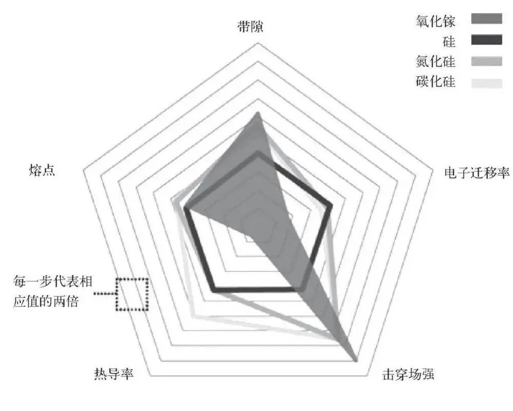
Comparison of physical properties of gallium oxide with silicon, silicon nitride and silicon carbide Image from: New Material Industry (Journal)
However, there is no rose without a thorn. On one hand, the mobility and thermal conductivity of gallium oxide are lower than that of silicon carbide and gallium nitride, which may be affected by the self-heating effect, resulting in the degradation of equipment performance; On the other hand, it is difficult to realize p-type doping, and it is difficult to manufacture p-type semiconductors, which has become the main obstacle to realize high-performance devices.
Fortunately, researchers found that when the temperature rises from room temperature to 250 ℃, the performance of devices made of gallium oxide will not decline significantly, and in practical applications, the temperature rarely exceed 250 ℃. And gallium oxide devices can be in very small size and thin, so even if the thermal conductivity is low, thermal management can be very effective. At the same time, the industry has designed a variety of device configurations, effectively avoiding the difficulty of p-type doping, and achieving good device performance.Although these two defects can be avoided, further discussion is still needed in practical application.Semiconductor devices made of gallium oxide can achieve more high voltage withstanding, smaller size and lower loss, so it has potential application value in photoelectric detection, power devices, radio frequency devices, gas sensing, photocatalysis, information storage and solar energy utilization. So far, the commercialization trend of gallium oxide is clear in the fields of solar blind ultraviolet photodetectors and power devices (SBD, MOSFET).
Difficulty in preparation
Since there are so many advantages, why hasn't it thrived yet? This is because the industrialization of gallium oxide has been stuck in the step of large-scale preparation. With the deepening of research and the clear application of devices, the road of industrialization is gradually paved.
The research of Ga2O3 is mainly application-oriented, and the conversion from Ga2O3 materials to chips is similar to the industrial system of silicon carbide--"substrate → epitaxy → device".
Substrate refers to the wafer made of semiconductor single crystal material. After careful processing such as cutting, grinding and polishing, it is the basic material polishing sheet for chip manufacturing; Epitaxy refers to the process of growing a new single crystal film on the polished single crystal substrate, and the epitaxial film is equivalent to the functional part of the semiconductor device; A device is a kind of chip that can realize specific functions. The wafer will first go through photolithography, etching, ion implantation, CMP, metallization, testing and other processes, and then go through complex processes such as cutting and packaging.
In this process, gallium oxide can be used as both substrate and epitaxial material.
According to its diameter, the wafer is sorted into 4 inches, 6 inches, 8 inches, 12 inches and so on. The chip is cut from the processed wafer. Wafer is round, while chip is square. That’s why it is only the larger wafer that can make more complete chips. The size of wafer and the manufacturing process are also closely bound up. At present, chips with 14nm or more advanced manufacturing process are basically made of 12-inch wafers, because the larger the wafer is, the less the substrate costs.
Therefore, only when gallium oxide is made into a certain size wafer can it be truly put into industrialization, and the size of the wafer will become larger.
Growth of Single Crystal
It is very difficult to produce β phase gallium oxide wafers with large size and high quality because melting point of its single crystal is high up to 1820 ℃. It is very easy to decompose and volatilize during growth process under the high temperature, and it is easy to produce a large number of oxygen vacancies, resulting in defects such as twinned, mosaic structure, spiral dislocation, etc. In addition, the gas, generated by decomposition at high temperature, such as GaO, Ga2O and Ga, will seriously corrode the iridium crucible.
The research on the growth of Ga2O3 single crystal can be traced back to the 1960s. The preparation methods mainly include Verneuil process, Czochralski method, edge-defined film-fed growth, floating zone method and Bridgman method.
At present, the Japanese NCT company, which develops best in this field in the world, is the main supplier of Ga2O3 substrates in the world. The company has successfully grown the largest 6-inch Ga2O3 single crystal by the edge-defined film-fed growth, while other methods are still unable to manufacture the large-size substrates required by the industry.
However, the gallium oxide produced by edge-defined film-fed growth has serious "precious metal dependence", and the crucible based on the precious metal iridium (Ir) needs to be used in the manufacturing process. Iridium is scarce in the world. The price of iridium per gram is up to thousands of yuan, about three times the price of gold. The price of only one crucible in the crystal growth equipment is more than 5 million yuan.
Cost has become a core concern for foreign industries. It is commonplace to reduce the cost of iridium crucibles by increasing the ingot size, improving the processing rate and extending the life of the crucible. A more thorough solution is to study other conversion method.
This is even more difficult for the domestic industries. China has the third largest reserves of gallium element in the world, with rich reserves of high-purity gallium oxide raw materials, and energy consumption of growth crystals could be reduced by 80%, and reached a yield of 50% or more, but China is not rich in iridium mineral resources. We are relying on imports, thus there is a risk of supply failure. To make matters worse, the crucible is easy to be damaged and has limited using times. Due to the high cost, it is hard to afford producing it; It is an endless loop.
The domestic research on the growth of Ga2O3 single crystal has only been carried out for more than ten years, and its maturity and stability are less than those of foreign industries. Research institutions such as China Electronics Technology 46 Institute, Xi'an University of Electronic Science and Technology, Shanghai Institute of Optics and Mechanics, Shanghai Institute of Microsystems, Fudan University, Nanjing University, Zhejiang University, etc. have developed growth technologies with independent intellectual property rights to fight against technological monopoly, but can only achieve substrate of up to 4 inches.
In order to gradually industrialize this technology, the main strategy in China is to reduce the use of precious metal iridium and promote the groping research of iridium-free process. This trend is becoming more and more obvious when the pace of industrialization is accelerating. The start-up company Evolusia announced that it has developed a unique technique "iridium-free method" to solve the cost obstacle ; In May 2022, the Hangzhou International Science and Technology Innovation Center of Zhejiang University announced that it had invented a new melt method to develop Ga2O3 bulk single crystals and wafers, reducing the use of precious metal iridium, and has successfully prepared Ga2O3 wafers with a diameter of 2 inches.
Thin film epitaxy
Epitaxial growth is one of the core processes for preparing semiconductor devices, which is closely related to device performance. When the substrate material and epitaxial material are both gallium oxide, the epitaxy is called homogeneous epitaxy, and on the contrary, heteroepitaxy.
Limited by the size, quality, electrical properties and other factors of Ga2O3 single crystal substrate, the current research on Ga2O3 epitaxial growth focuses on heteroepitaxy, and the few homogeneous epitaxy is also based on the (100) substrate with the most stable and strongest cleavage surface.
At present, epitaxial thin film deposition technologies for Ga2O3 include molecular beam epitaxy (MBE), molecular organic vapor deposition (MOCVD), mist chemical vapor deposition (mist-CVD), and halide vapor epitaxy deposition (HVPE).
There are two mainstream technologies in the world: EFG of NCT combined with HVPE technology and CZ combined with MOVPE technology of IKZ Institute. However, in the competition, EFG produces a larger crystal size than Cz, and the epitaxial deposition rate of HVPE is about 10 times that of MOVPE. Therefore, EFG combined with HVPE technology has become the mainstream and realized industrialization.
Although the preparation technology of bulk Ga2O3 single crystal has made significant progress in China, the epitaxial technology of Ga2O3 in China is relatively weak. CETCA 46 Institute is the leading domestic Ga2O3 technology. In 2019, CETCA 46 Institute prepared a 4-inch Ga2O3 wafer using the edge-defined film-fed growth method. In December 2021, it successfully prepared a HVPE Ga2O3 homogeneous epitaxial wafer, breaking through the problems of vapor phase nucleation and quality of epitaxial layer in the process of HVPE homogeneous epitaxial Ga2O3, and filling the domestic gap.
Device application
Producing wafers does not mean everything is fine. There are also many obstacles remaining unsolved.Due to the brittleness of gallium oxide crystals, easy-cleavage properties and low fracture toughness, the traditional grinding processing is easy to produce cracks and pit defects on the surface. A series of process research will be involved in the ultra-precision processing of wafers, including grinding and polishing, and the industrialization process will drive the whole chain.
In terms of device application, the early stage of single crystal growth of gallium oxide is mainly aimed at solar blind deep ultraviolet detector. In 2012, when gallium oxide homogeneous epitaxial wafer was applied to power devices, a new era of industrialization was officially started.
At present, the research of gallium oxide focuses on the Schottky barrier diode (SBD) and metal-oxide semiconductor field effect transistor (MOSFET), and by enhancing the device structure, the breakdown voltage value is constantly refreshed.
In terms of device development, Japan started early, Mitsubishi Heavy Industries, Toyota, Denso, Tamura Manufacturing (established NCT in cooperation with NICT), KOHA Co., Ltd and other enterprises have long been involved in development and layout of gallium oxide industry, with a rapid development trend. The United States is relatively slow, with Kyma launching a 1-inch gallium oxide wafer in 2020.
Among domestic leading gallium oxide devices, the ones belong to the 13th Institute of China Electronics Technology Group Corporation stand at the front of the industry. The threshold voltage of enhanced MOSFET gallium oxide device, which is realized by thermal oxidation technology, reaches 4.1V and its switch ratio reaches 108. The proposed double-layer source field board structure can effectively inhibit the peak electric field strength in the gallium oxide channel and silicon nitride (SiN) passivation layer, and the breakdown voltage of the device exceeds 3000V.
Domestic investment and financing began to surge
Gallium oxide is a promising business in the next decade, and industry analysts say the global market for gallium oxide and power devices is expected to reach 9.86 billion yuan by 2030.In terms of industrialization, domestic industries have just started, but many investment funds have begun to pay attention to the future of gallium oxide, seeking related entrepreneurial projects and entrepreneurial teams to promote the development of gallium oxide in China. Beijing Gallium Family Technology, Hangzhou Fujia Gallium Technology, Beijing MIGSEMI , Shenzhen Evolusia are the four active companies currently in the investment and financing market.
According to estimation from the China Electronic News, the two main direction of gallium oxide are radiation detection sensor chip and power correction, inverter, high power as well as high power chip, which will play an important role especially in ultra wide band system available power and voltage range, including application scenarios such as power regulation and high voltage rectifier of distribution system, electric vehicles and photovoltaic solar energy system.
Xu Zhaoyuan, CEO of Evolusia, said in an interview with 36 Kr that research and development of silicon carbide has been carrying on for 40 years, while gallium oxide only 10 years. Gallium oxide, which moves along the course of silicon carbide, is likely to follow a similar development trend: first rooting in the field of fast charging and industrial power supply with low market threshold, and then booming in the automotive field.
Gallium oxide has made significant progress in the last decade, which is just one step away from the industrialization. Meanwhile, the research on material preparation and related properties is still not systematic and in-depth. To dominate the future, the present decade is crucial.
