Paper Sharing
【Domestic Papers】Songshan Lake Materials Laboratory---Deep UV Detection: from Single-crystalline MgZnO to Amorphous Ga₂O₃
日期:2025-05-08阅读:884
Researchers from the Songshan Lake Materials Laboratory have published a dissertation titled " Deep UV Detection: from Single-crystalline MgZnO to Amorphous Ga2O3" in CHINESE JOURNAL OF LUMINESCENCE.
Background
Solar-blind ultraviolet (UV) detection (220-280 nm) holds significant value in military, civil security, communication, medical, and other fields due to its effective elimination of solar background interference. Traditional detectors (e.g., photomultiplier tubes, silicon photodiodes with filters) suffer from drawbacks like large volume, need for high voltage, fragility, or requirement for filters and limited sensitivity. Wide-bandgap semiconductors (e.g., Diamond, AlGaN, MgZnO, Ga2O3) provide the material basis for developing filterless, compact solid-state solar-blind detectors. AlGaN technology is relatively mature but costly and involves complex processes; MgZnO allows for solar-blind detection by adjusting Mg composition, but faces challenges like phase separation within the required composition range and difficulties in p-type doping. Ga2O3 (bandgap ~4.9 eV) is a natural solar-blind detection material, offering stability and low cost. Amorphous Ga2O3 (a-Ga2O3) presents outstanding advantages such as low-temperature, large-area fabrication, compatibility with flexible substrates, low-cost preparation methods, exhibits excellent detection performance, and holds great potential for industrialization.
Abstract
Wide bandgap semiconductors have great potential for the development of compact solar-blind ultraviolet detectors without filters. This article summarizes the research progress of deep ultraviolet photodetectors using wide bandgap oxide semiconductors including MgZnO and amorphous Ga2O3(a-Ga2O3) thin films. It has been found that the photoresponse performance of a-Ga2O3 thin film is comparable or even better than that of crystalline thin films. Numerous results demonstrate that oxygen vacancy (VO) defects play a crucial role in device performance. Based on the effective modulation of VO defects, high performance solar-blind ultraviolet photodetectors can be successfully achieved. In addition, the persistent photoconductivity effect, which is usually accompanied by the presence of VO defects in oxide materials, provides a new perspective for the development of optoelectronic synaptic devices in deep ultraviolet range. Finally, a brief discussion is provided concerning the above research progress as well as some unsolved issues. These advancements are expected to promote the industrial application of wide bandgap oxide semiconductor materials, especially a-Ga2O3, in deep ultraviolet detection in the future.
Conclusion
Wide-bandgap semiconductors MgZnO and Ga2O3 are ideal materials for filterless deep UV detectors. The research history shows that defects, not just crystalline quality, play a crucial role in controlling the performance of oxide semiconductor detectors. Amorphous Ga2O3 thin films, leveraging unique defect-related gain mechanisms, exhibit DUV photoresponse characteristics comparable or superior to single-crystal films. Oxygen vacancies (VO) are key defects in amorphous Ga2O3, and their effective modulation is central to optimizing device performance. The persistent photoconductivity (PPC) effect caused by Vo opens new opportunities for amorphous Ga2O3 in novel devices like optoelectronic synapses and memory. Despite significant progress, challenges remain in comprehensive performance improvement (balancing responsivity and speed), deep understanding of defect physics in amorphous materials, innovative device design, and application-specific optimization. Amorphous Ga2O3 material holds great promise for future industrial applications in deep UV detection and related optoelectronics due to its excellent performance potential, low cost, and simple fabrication advantages.
Graphic
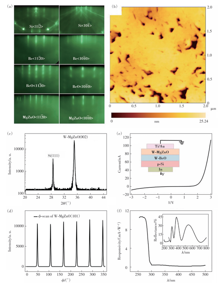
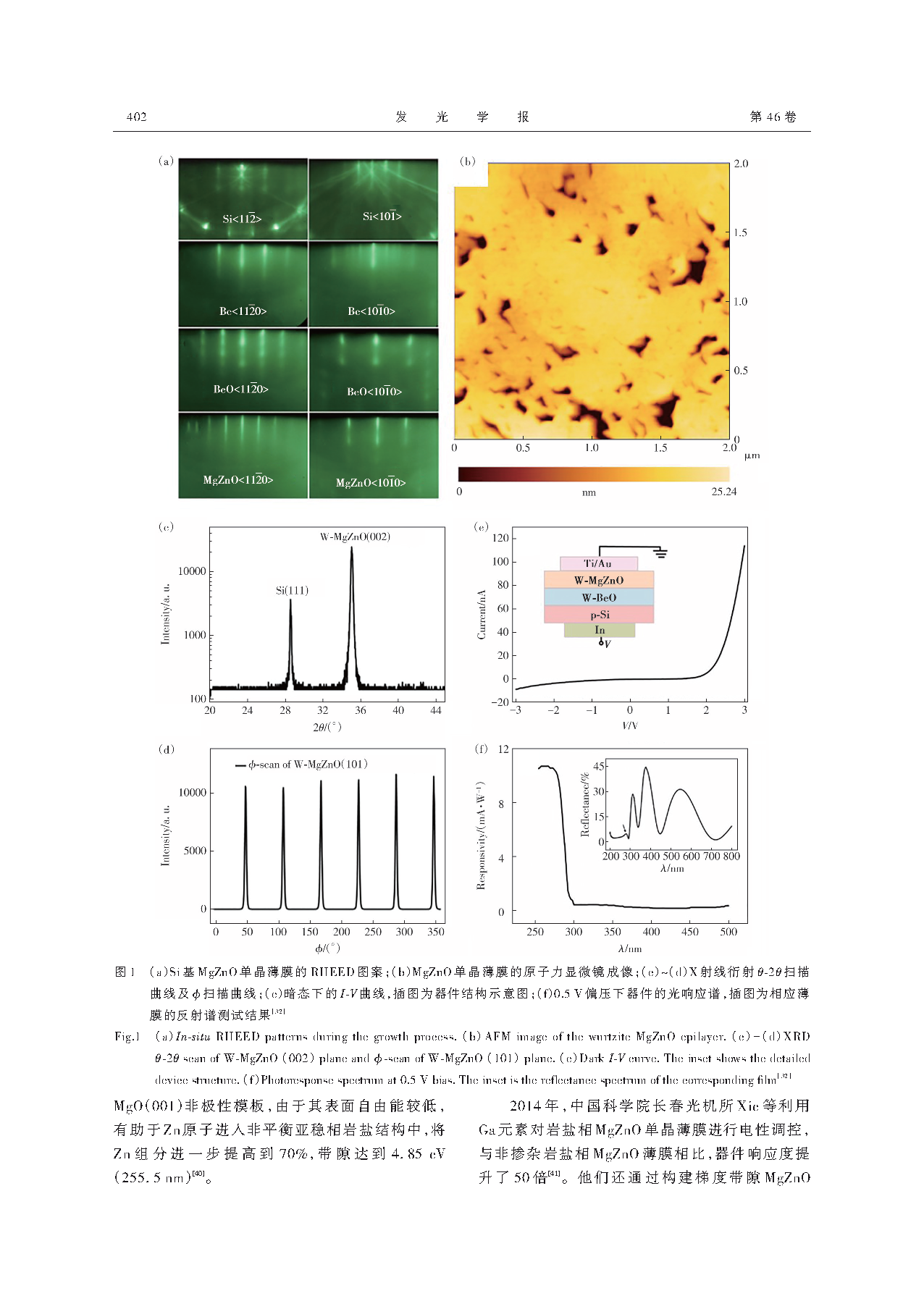
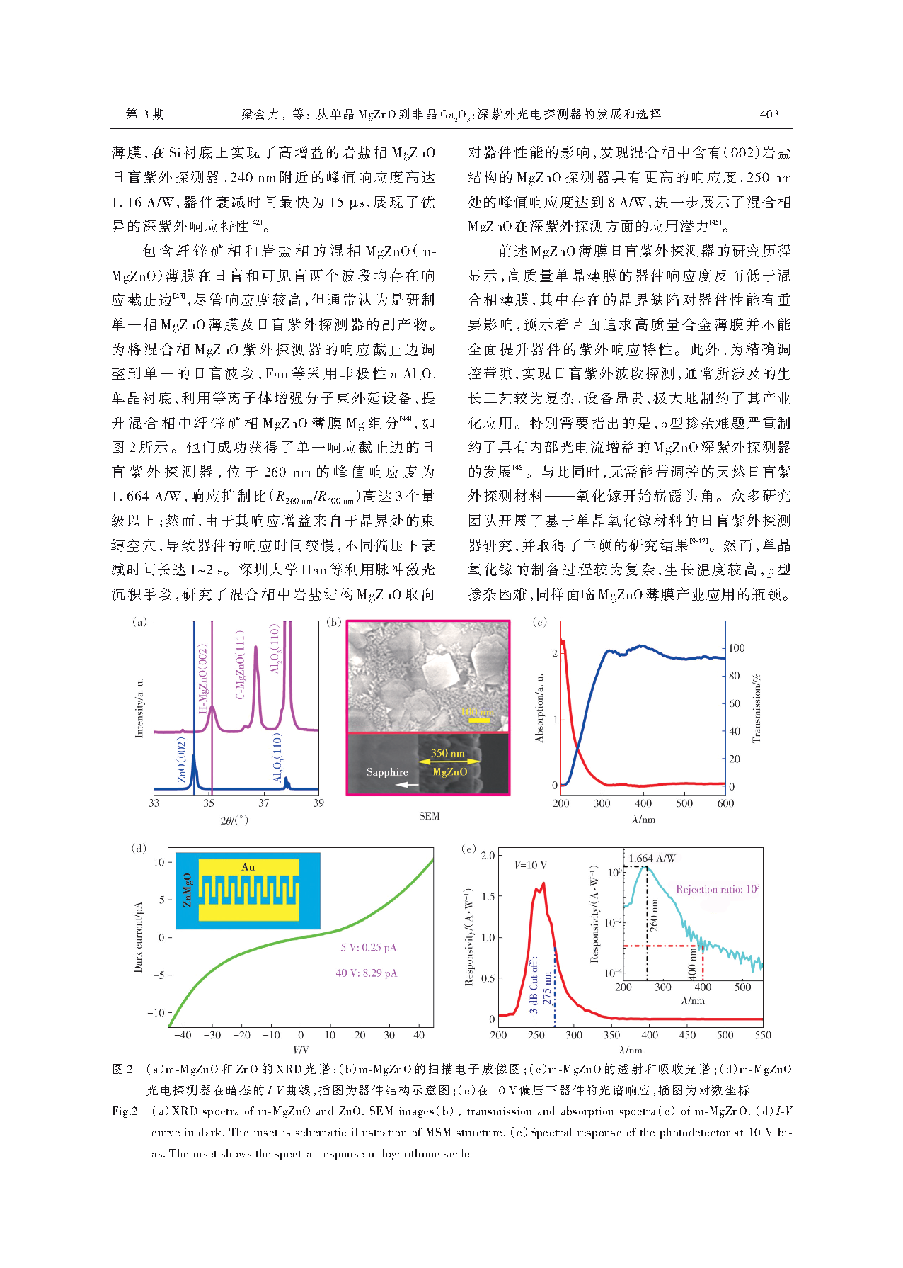
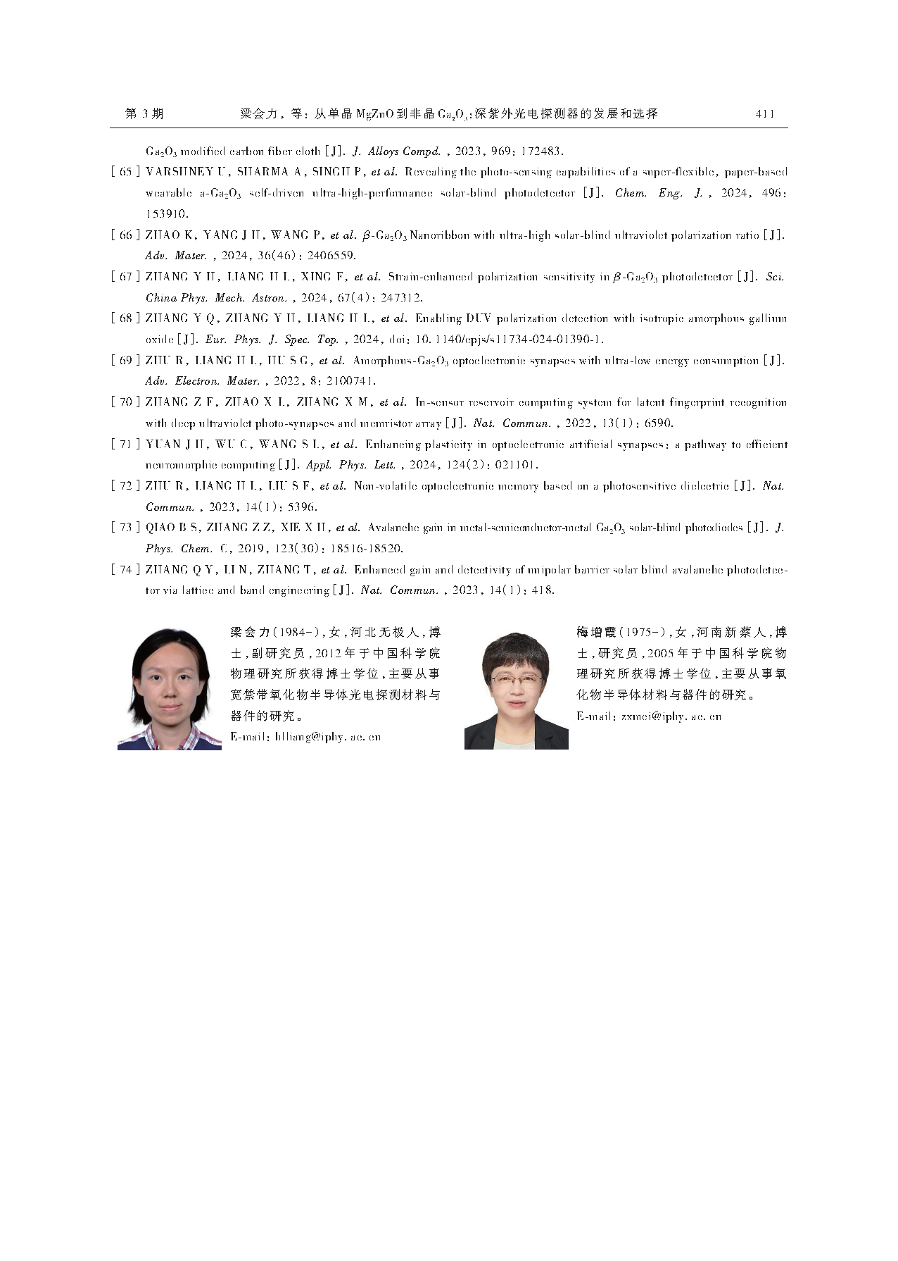
Fig.1 (a)In-situ RHEED patterns during the growth process.(b)AFM image of the wurtzite MgZnO epilayer.(c)-(d)XRD θ-2θ scan of W-MgZnO (002) plane and ϕ-scan of W-MgZnO (101) plane.(e)Dark I-V curve. The inset shows the detailed device structure.(f)Photoresponse spectrum at 0.5 V bias. The inset is the reflectance spectrum of the corresponding film.
Fig.2 (a)XRD spectra of m-MgZnO and ZnO. SEM images(b), transmission and absorption spectra(c)of m-MgZnO.(d)I-V curve in dark. The inset is schematic illustration of MSM structure.(e)Spectral response of the photodetector at 10 V bi‐ as. The inset shows the spectral response in logarithmic scale.
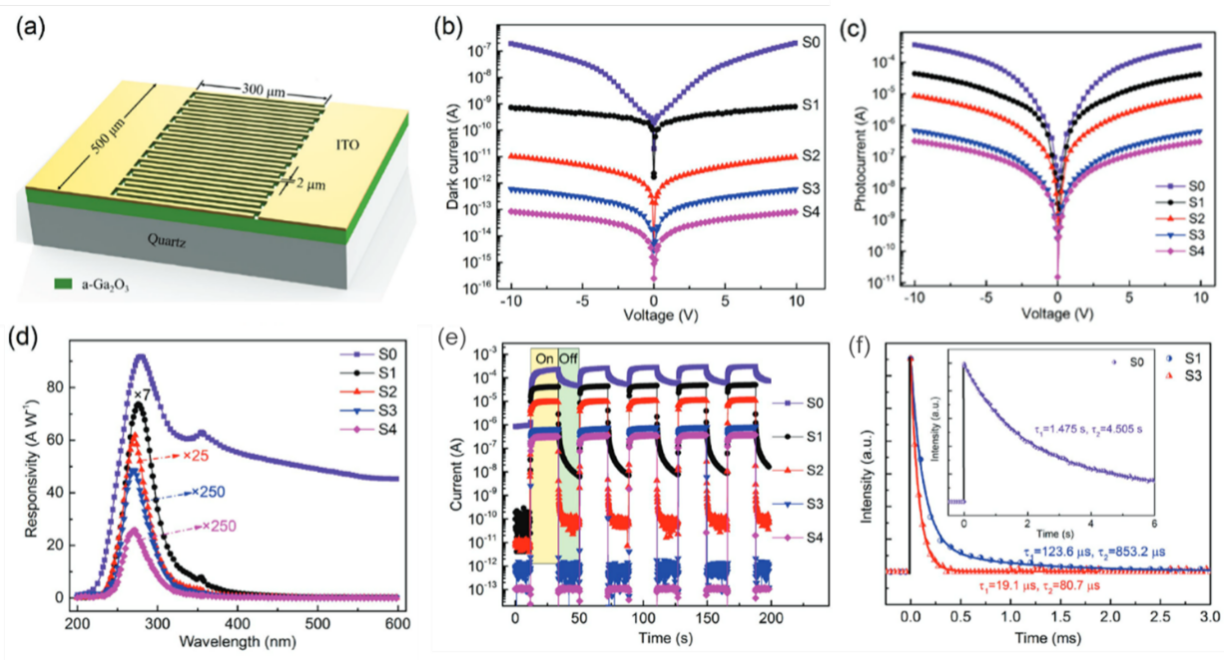
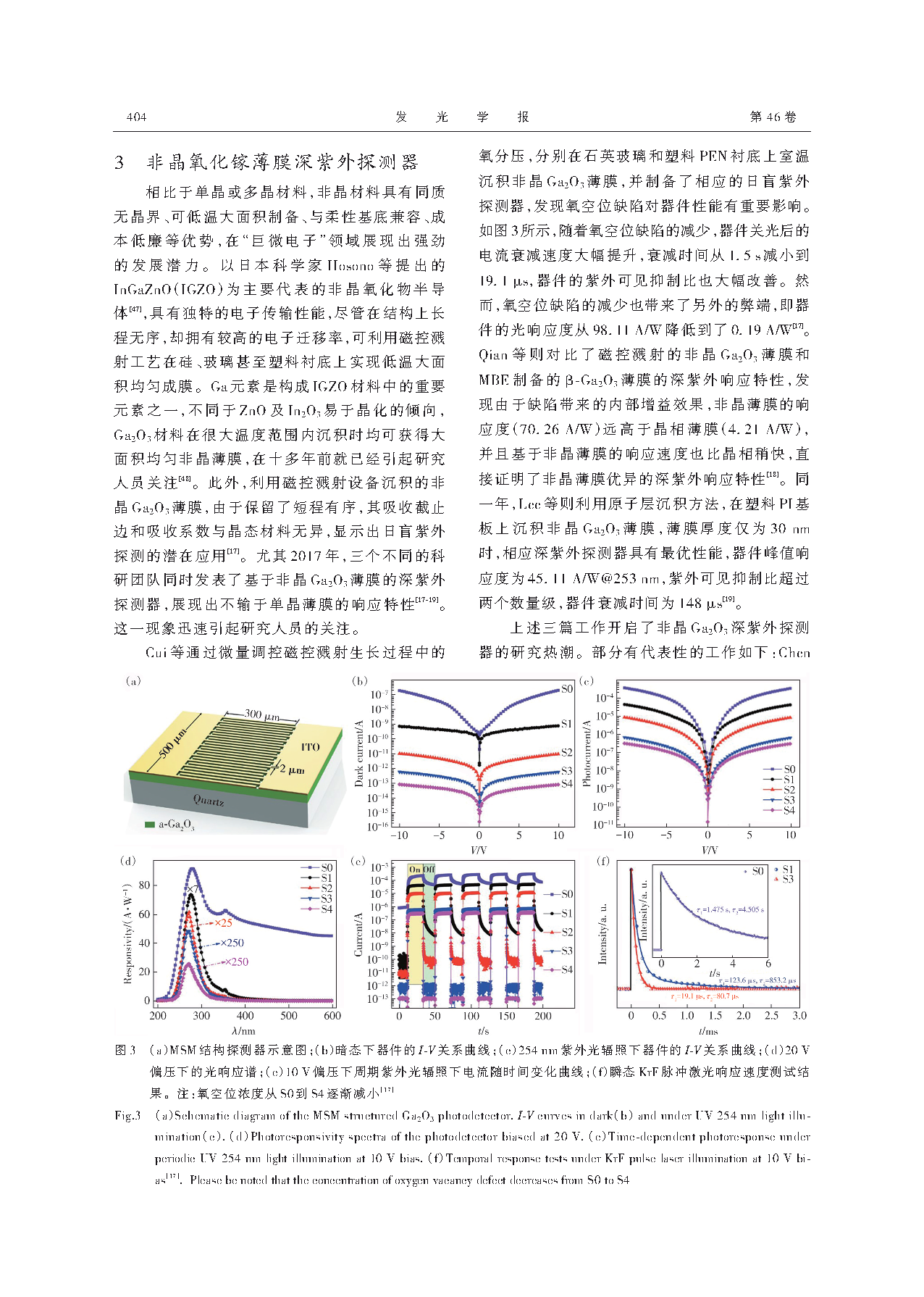
Fig. 3 (a) Schematic diagram of the MSM structured Ga2O3 photodetector. (b) I–V curves in dark and c) under UV 254 nm light illumination. d) Photoresponsivity spectra of the photodetector biased at 20 V. (e) Time-dependent photoresponse under periodic UV 254 nm light illumination at 10 V bias. (f) Temporal response tests under KrF pulse laser illumination at 10 V bias.
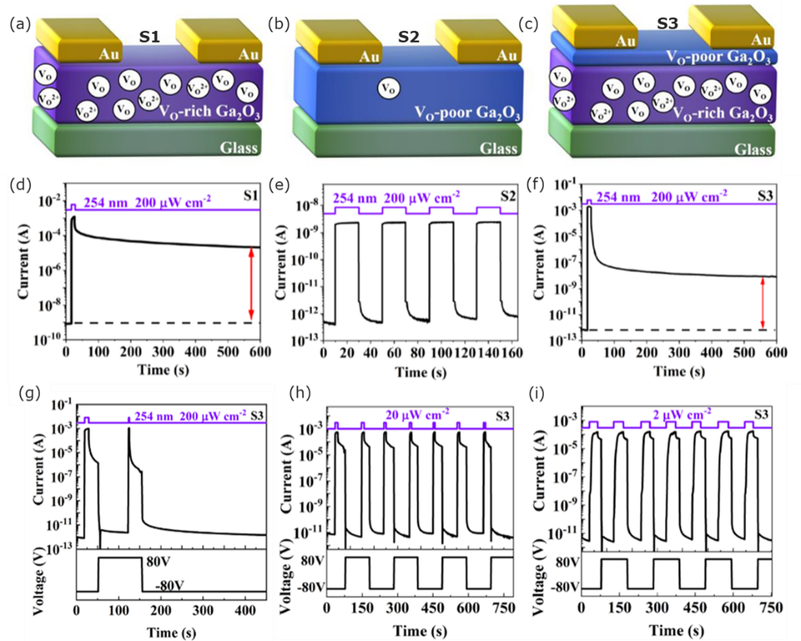
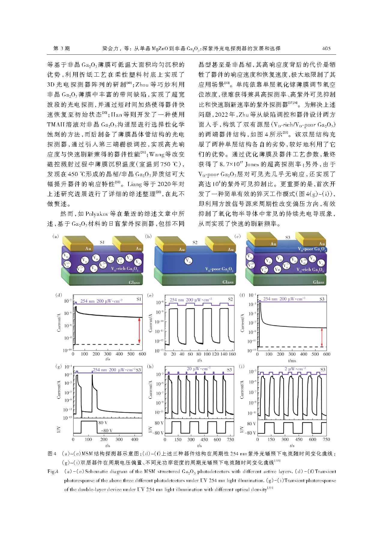
Fig. 4 (a)-(c) Schematic diagram of the MSM structured Ga2O3 photodetectors with different active layers. (d)-(f) Transient photoresponse of the above three different photodetectors under UV 254 nm light illumination. (g)-(i) Transient photoresponse of the double-layer device under UV 254 nm light illumination with different optical density.
DOI:
doi.org/10. 37188/CJL. 20240266