Paper Sharing
【Member Papers】Band Alignment, Thermal Transport Property, and Electrical Performance of High-Quality β-Ga₂O₃/AlN Schottky Barrier Diode Grown via MOCVD
日期:2025-05-08阅读:895
Researchers from the Fudan University and Suzhou Institute of Nano-Tech and Nano-Bionics,CAS have published a dissertation titled "Band Alignment, Thermal Transport Property, and Electrical Performance of High-Quality β-Ga2O3/AlN Schottky Barrier Diode Grown via MOCVD" in ACS Applied Materials & Interfaces.
Project Support
This work is supported by the National Key R&D Program of China (2023YFB4606300), National Natural Science Foundation of China (No. 62474049), the Science and Technology Innovation Plan of Shanghai Science and Technology Commission (Nos. 21DZ1100800, 23ZR1405300, 20501110700, and 20501110702), and the Joint Research Plan of sci-tech innovation community in Yangtze River Delta (No.2023CSJG0600). The authors also acknowledge Autinst Technology Co., Ltd for providing Autinst PIONEER-ONE TDTR measurements and technological help regarding this study. Part of the sample fabrication and experimental work was performed at Fudan Nanofabrication Laboratory.
Background
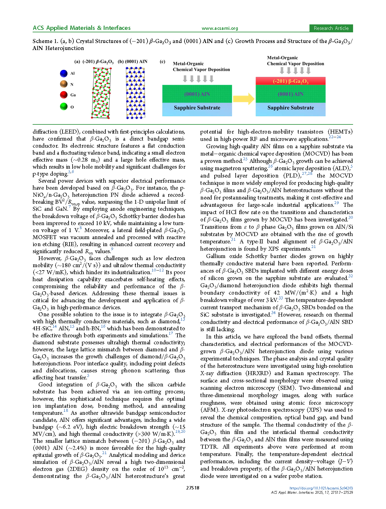
In recent years, the ultrawide-bandgap semiconductor β-phase gallium oxide (β-Ga2O3) has garnered significant attention due to its exceptional properties, including a wider bandgap (4.5− 4.9 eV) compared to Si, GaN, and SiC, an extremely high critical breakdown field (∼8 MV/cm), an outstanding Baliga’s figure of merit (BFOM ∼2800), and a high electron saturation velocity (∼2 × 107 cm/s). β-Ga2O3 has a promising future to be applied to high-voltage power devices. Among all crystal structures of gallium oxide (α, β, γ, δ, and ε phases), β-phase gallium oxide exhibits the highest thermal and chemical stability. Additionally, the production cost of large-size bulk crystals of β-Ga2O3 is significantly lower than that of other wide-bandgap materials. The β-Ga2O3 unit cell adopts a monoclinic crystal structure (C2/m space group) with lattice parameters of a = 12.23 Å, b = 3.04 Å, and c = 5.80 Å. Its structure comprises GaO6 octahedra and GaO4 tetrahedra.
Experimental measurements, including angle-resolved photoelectron spectroscopy (ARPES) and low-energy electron diffraction (LEED), combined with first-principles calculations, have confirmed that β-Ga2O3 is a direct bandgap semiconductor. Its electronic structure features a flat conduction band and a fluctuating valence band, indicating a small electron effective mass (∼0.28 m0) and a large hole effective mass, which results in low hole mobility and significant challenges for p-type doping.
Several power devices with superior electrical performance have been developed based on β-Ga2O3. For instance, the p-NiOx/n-Ga2O3 heterojunction PN diode achieved a recordbreaking BV2 /Ron,sp value, surpassing the 1-D unipolar limit of SiC and GaN. By employing anode engineering techniques, the breakdown voltage of β-Ga2O3 Schottky barrier diodes has been improved to exceed 10 kV, while maintaining a low turnon voltage of 1 V. Moreover, a lateral field-plated β-Ga2O3 MOSFET was vacuum annealed and processed with reactive ion etching (RIE), resulting in enhanced current recovery and significantly reduced Ron values.
However, β-Ga2O3 faces challenges such as low electron mobility (∼180 cm2 /(V s)) and ultralow thermal conductivity (<27 W/mK), which hinder its industrialization. Its poor heat dissipation capability exacerbates self-heating effects, compromising the reliability and performance of the β-Ga2O3-based devices. Addressing these thermal issues is critical for advancing the development and application of β-Ga2O3 in high-performance devices.
Abstract
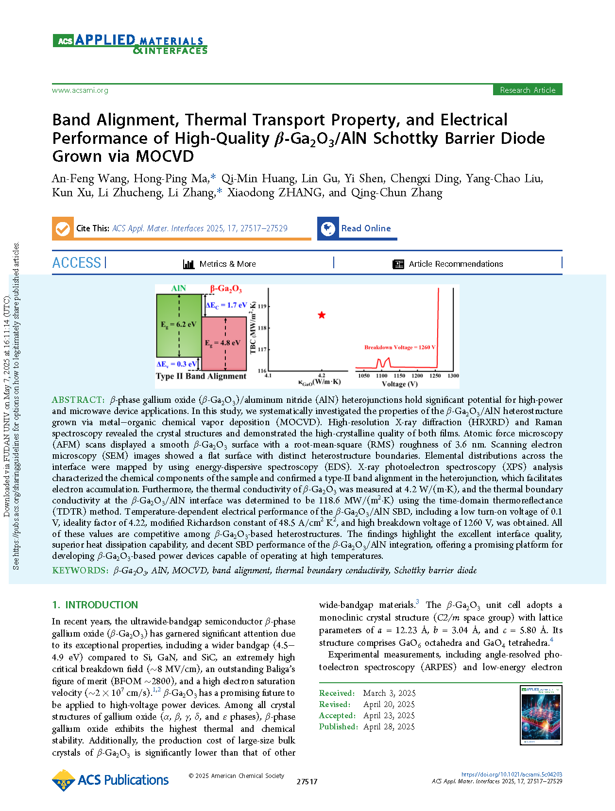
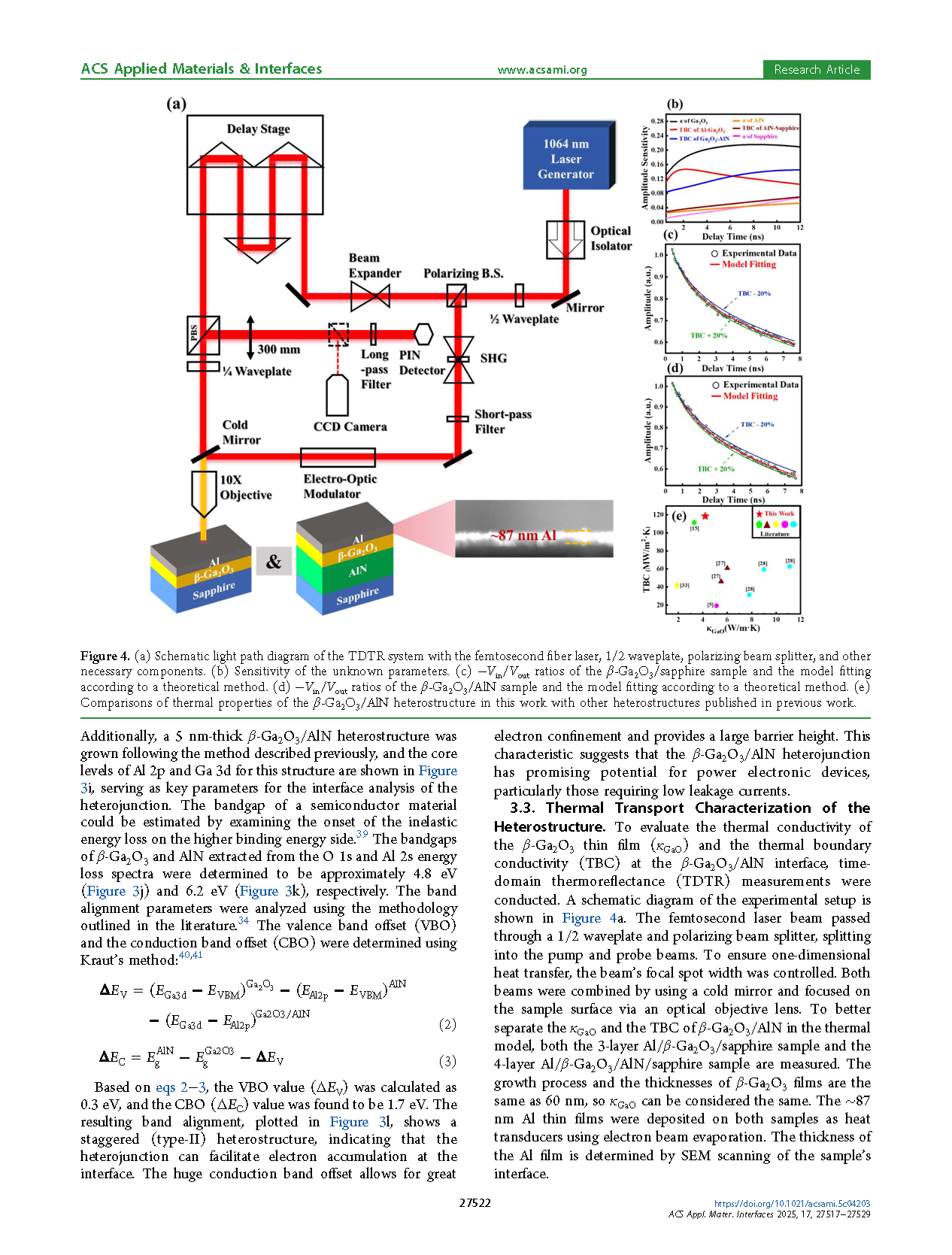
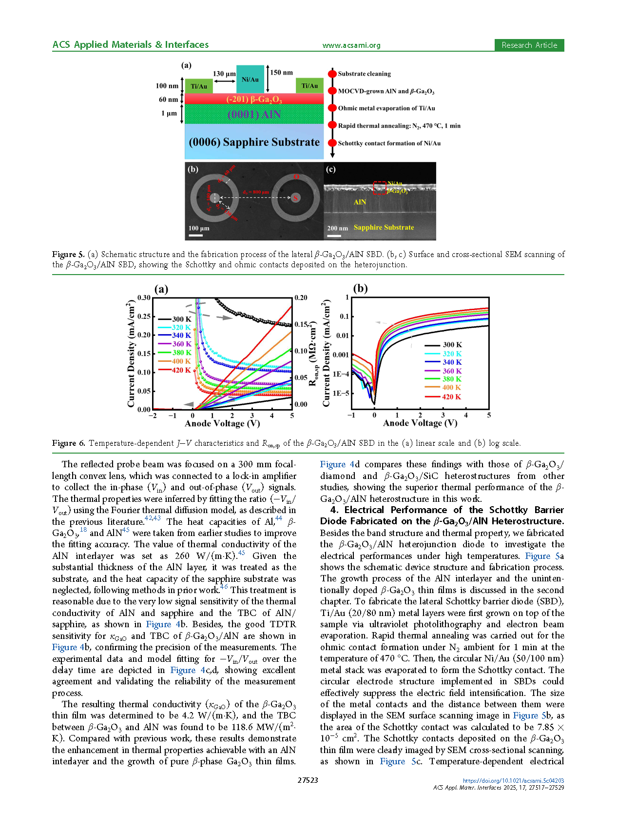
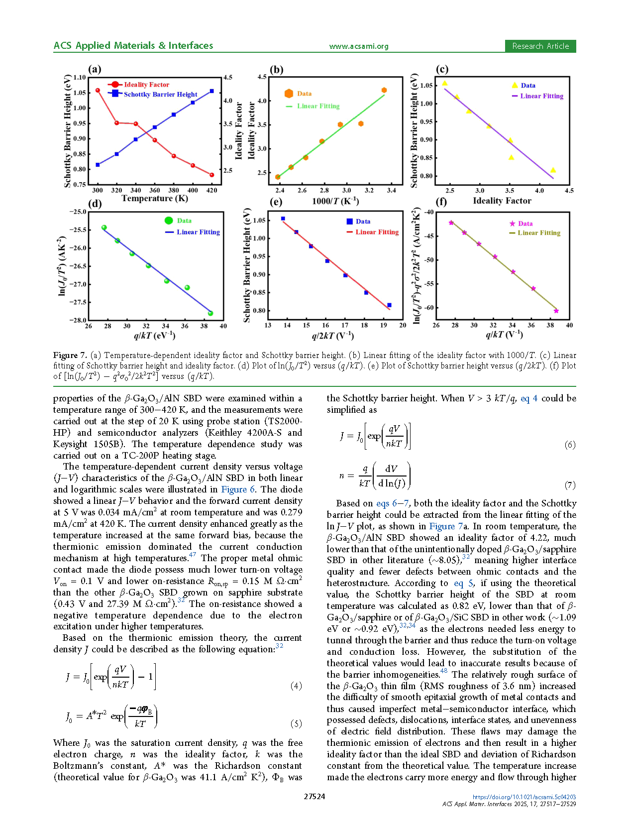
β-phase gallium oxide (β-Ga2O3)/aluminum nitride (AlN) heterojunctions hold significant potential for high-power and microwave device applications. In this study, we systematically investigated the properties of the β-Ga2O3/AlN heterostructure grown via metal–organic chemical vapor deposition (MOCVD). High-resolution X-ray diffraction (HRXRD) and Raman spectroscopy revealed the crystal structures and demonstrated the high-crystalline quality of both films. Atomic force microscopy (AFM) scans displayed a smooth β-Ga2O3 surface with a root-mean-square (RMS) roughness of 3.6 nm. Scanning electron microscopy (SEM) images showed a flat surface with distinct heterostructure boundaries. Elemental distributions across the interface were mapped by using energy-dispersive spectroscopy (EDS). X-ray photoelectron spectroscopy (XPS) analysis characterized the chemical components of the sample and confirmed a type-II band alignment in the heterojunction, which facilitates electron accumulation. Furthermore, the thermal conductivity of β-Ga2O3 was measured at 4.2 W/(m·K), and the thermal boundary conductivity at the β-Ga2O3/AlN interface was determined to be 118.6 MW/(m2·K) using the time-domain thermoreflectance (TDTR) method. Temperature-dependent electrical performance of the β-Ga2O3/AlN SBD, including a low turn-on voltage of 0.1 V, ideality factor of 4.22, modified Richardson constant of 48.5 A/cm2 K2, and high breakdown voltage of 1260 V, was obtained. All of these values are competitive among β-Ga2O3-based heterostructures. The findings highlight the excellent interface quality, superior heat dissipation capability, and decent SBD performance of the β-Ga2O3/AlN integration, offering a promising platform for developing β-Ga2O3-based power devices capable of operating at high temperatures.
Summary
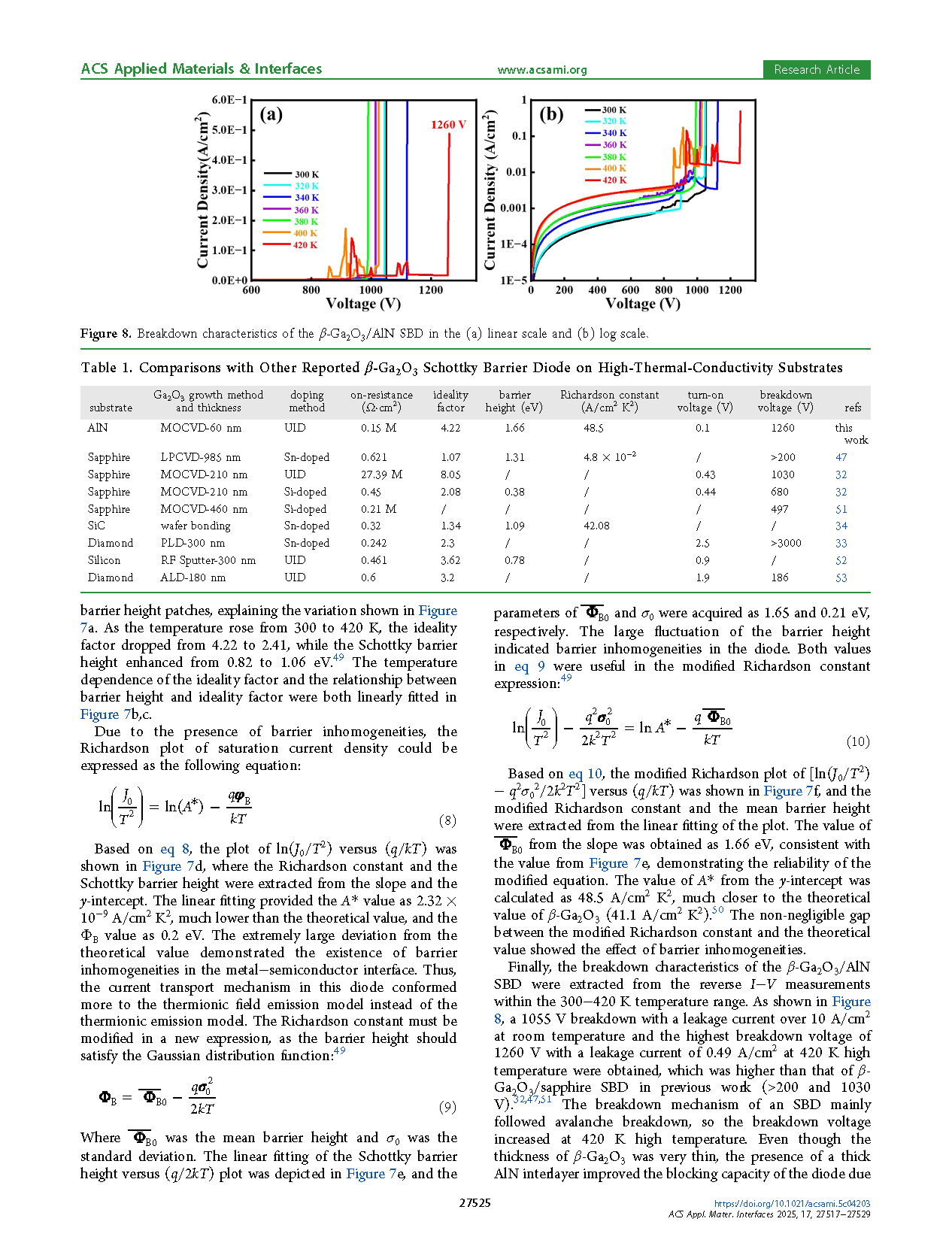
In this study, a high-quality β-Ga2O3/AlN heterostructure was successfully grown by using the MOCVD method. The physical and optical properties, band alignment, and thermal characteristics of the heterojunction were thoroughly analyzed. The as-grown heterostructure exhibited high crystal quality, a low surface roughness of 3.6 nm, and a well-integrated boundary. XPS survey spectra confirmed the presence of distinct components within the sample, while core-level, VBM, and energy loss spectral measurements revealed a type-II band alignment of the β-Ga2O3/AlN interface. The thermal conductivity of β-Ga2O3 was measured at 4.2 W/(m·K), and the thermal boundary conductivity at the β-Ga2O3/AlN interface was found to be 118.6 MW/(m2·K), highlighting the efficient heat dissipation enabled by the AlN interlayer and the high-quality growth of the heterostructure. The β-Ga2O3/ AlN Schottky barrier diode was fabricated and the electrical performances of a low turn-on voltage of 0.1 V, ideality factor of 4.22, modified Richardson constant of 48.5 A/cm2 K2, and a high breakdown voltage over 1.2 kV at high temperature were measured, showing good capability and potential of the β-Ga2O3/AlN SBD to operate under extreme thermal environments.
These findings demonstrate the potential of β-Ga2O3/AlN heterostructures as an innovative solution for power devices that require enhanced thermal management, especially in hightemperature environments. The results open the door to the development of advanced power devices with improved performance and reliability. Future research will focus on fabricating a new β-Ga2O3/AlN power device with lower on resistance, ideality factor, and barrier inhomogeneities while maintaining high heat-sinking capability and excellent breakdown characteristics. Its practical applications in power and RF electronics are also of great interest.
Graphic
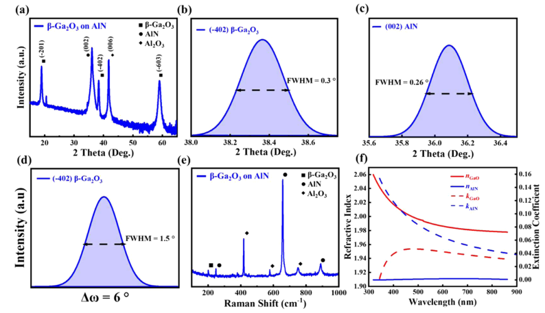
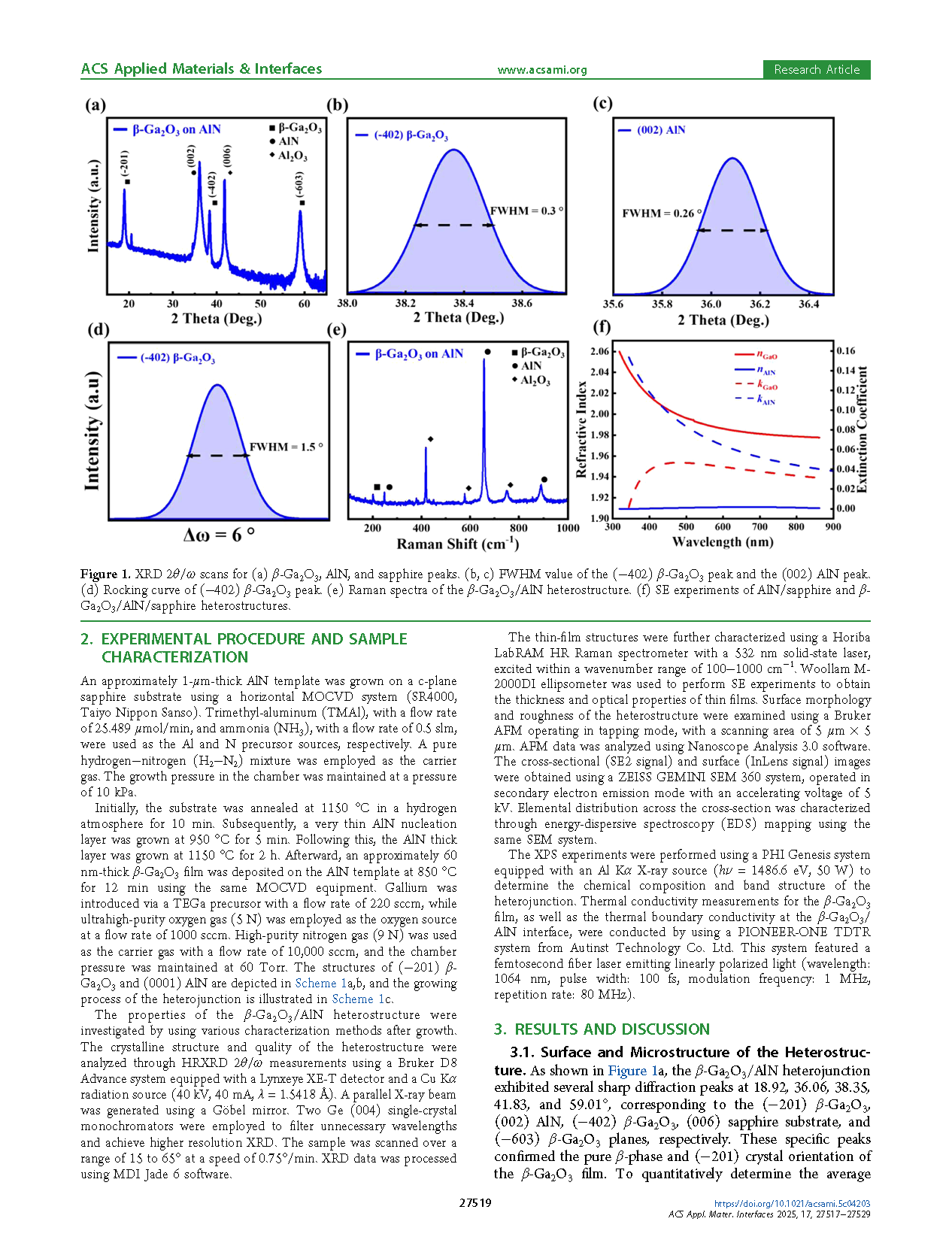
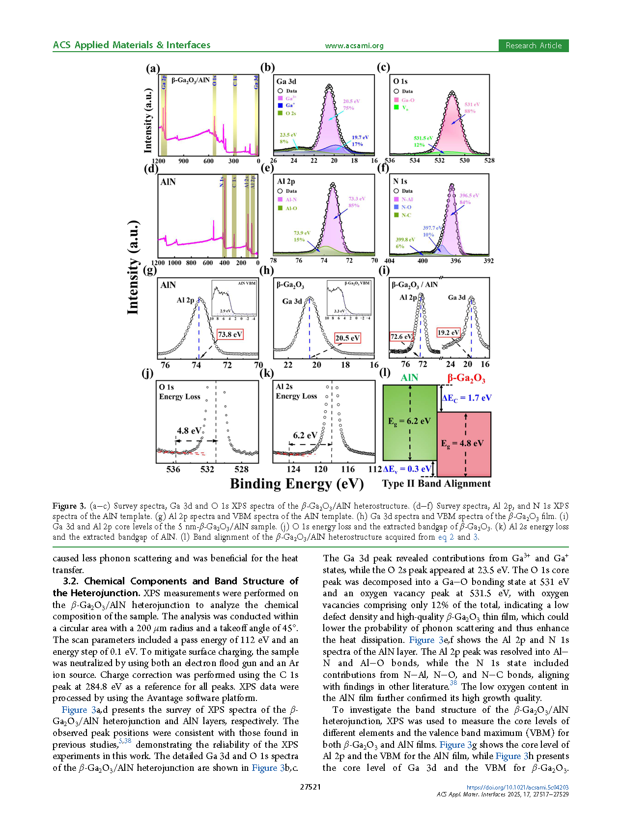
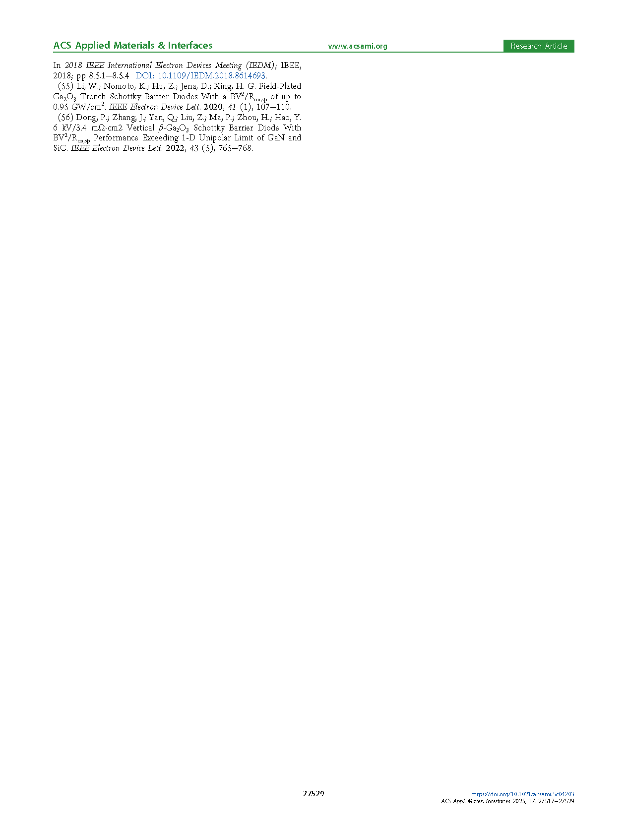
Figure 1. XRD 2θ/ω scans for (a) β-Ga2O3, AlN, and sapphire peaks. (b, c) FWHM value of the (−402) β-Ga2O3 peak and the (002) AlN peak. (d) Rocking curve of (−402) β-Ga2O3 peak. (e) Raman spectra of the β-Ga2O3/AlN heterostructure. (f) SE experiments of AlN/sapphire and β-Ga2O3/AlN/sapphire heterostructures.
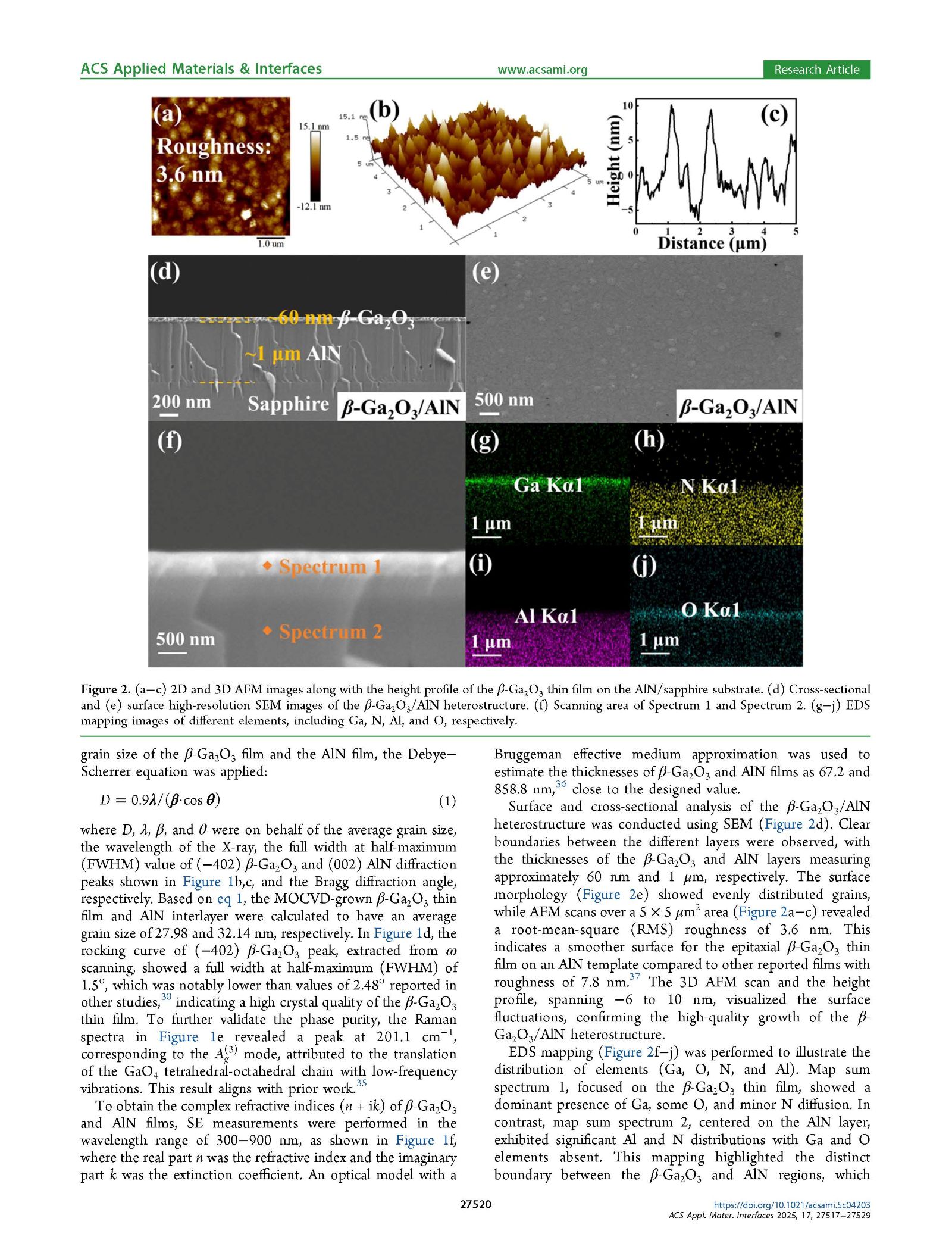
Figure 2. (a−c) 2D and 3D AFM images along with the height profile of the β-Ga2O3 thin film on the AlN/sapphire substrate. (d) Cross-sectional and (e) surface high-resolution SEM images of the β-Ga2O3/AlN heterostructure. (f) Scanning area of Spectrum 1 and Spectrum 2. (g−j) EDS mapping images of different elements, including Ga, N, Al, and O, respectively.
DOI:
doi.org/10.1021/acsami.5c04203,