Paper Sharing
【Domestic Papers】Shanghai Microwave Technology Research Institute---Effect of Rapid Thermal Annealing on the Characteristics of Micro Zn-Doped Ga₂O₃ Films by Using Mixed Atomic Layer Deposition
日期:2025-05-12阅读:962
Researchers from the Shanghai Microwave Technology Research Institute have published a dissertation titled "Effect of Rapid Thermal Annealing on the Characteristics of Micro Zn-Doped Ga2O3 Films by Using Mixed Atomic Layer Deposition" in Nanomaterials.
Funding
The presented work is supported by the Shanghai Sailing Program (Nos. 22YF1446200, 23YF1444300), Shanghai Super Postdoctoral Plans Encouragement Programs (No. 2023078). This work is also supported by the Anhui University Provincial Natural Science Research Project, China (KJ2021A1089), Research Initiation Fund Project of Chuzhou University (2023qd94).
Abstract
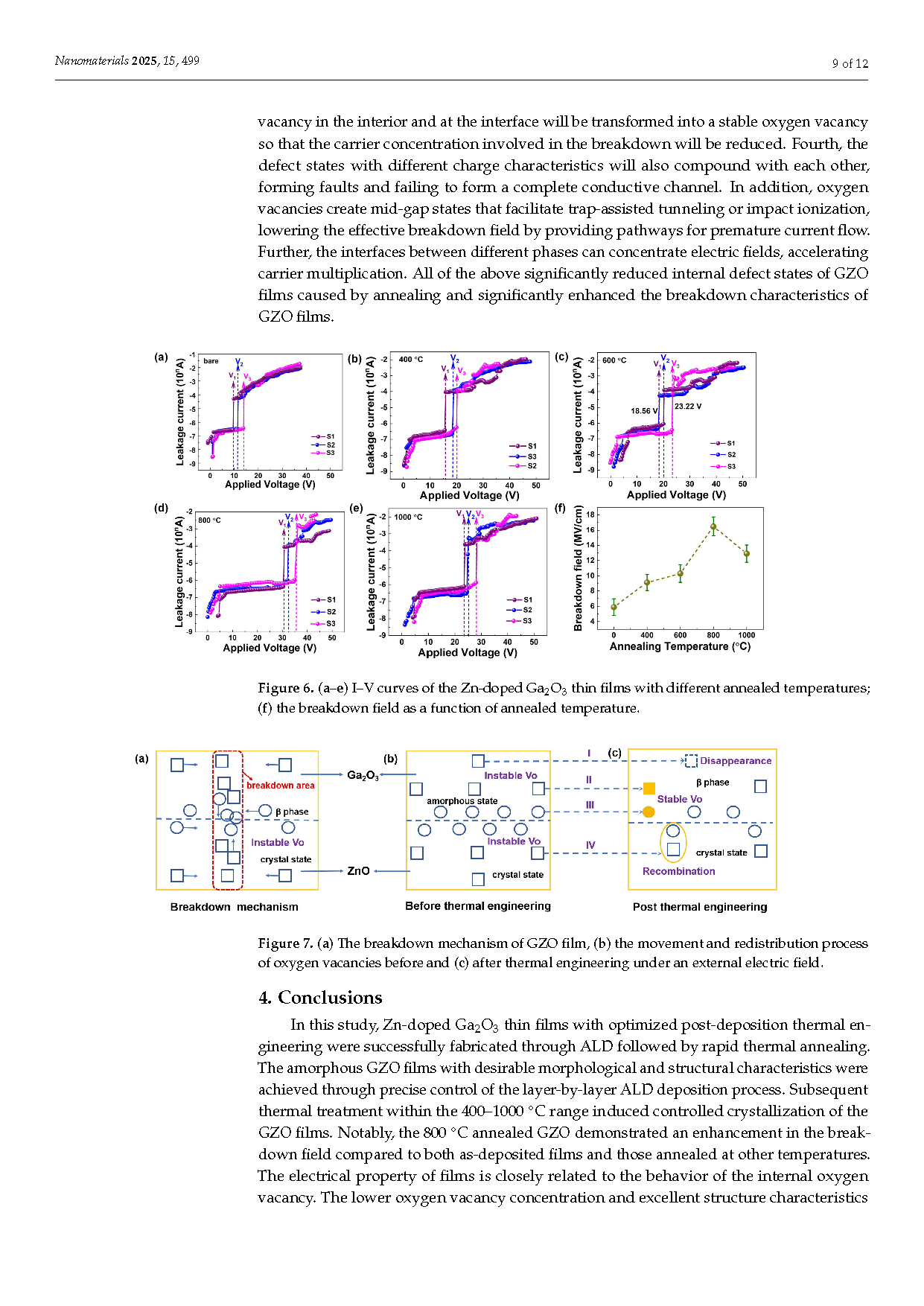
In this work, micro Zn-doped Ga2O3 films (GZO) were deposited by one-step mixed atomic layer deposition (ALD) followed by post-thermal engineering. The effects of Zn doping and post-annealing temperature on both structure characteristics and electric properties were investigated in detail. The combination of plasma-enhanced ALD of Ga2O3 and thermal ALD of ZnO can realize the fast growth rate (0.62 nm/supercyc.), high density (4.9 g/cm3), and smooth interface (average Rq = 0.51 nm) of Zn-doped Ga2O3 film. In addition, the thermal engineering of the GZO was achieved by setting the annealing temperature to 400, 600, 800, and 1000 °C, respectively. The GZO film annealed at 800 °C exhibits a typical crystalline structure (Ga2O3: β phase, ZnO: hexagonal wurtzite), a lower roughness (average Rq = 2.7 nm), and a higher average breakdown field (16.47 MV/cm). Notably, compared with the pure GZO film, the breakdown field annealed at 800 °C increases by 180%. The OV content in the GZO after annealing at 800 °C is as low as 34.8%, resulting in a remarkable enhancement of electrical properties. These research findings offer a new perspective on the high-quality ALD-doped materials and application of GZO in high-power electronics and high-sensitive devices.
Conclusions
In this study, Zn-doped Ga2O3 thin films with optimized post-deposition thermal engineering were successfully fabricated through ALD followed by rapid thermal annealing. The amorphous GZO films with desirable morphological and structural characteristics were achieved through precise control of the layer-by-layer ALD deposition process. Subsequent thermal treatment within the 400–1000 °C range induced controlled crystallization of the GZO films. Notably, the 800 °C annealed GZO demonstrated an enhancement in the breakdown field compared to both as-deposited films and those annealed at other temperatures. The electrical property of films is closely related to the behavior of the internal oxygen vacancy. The lower oxygen vacancy concentration and excellent structure characteristics of GZO annealing at 800 °C significantly improved the breakdown characteristics of the MOS device. Moreover, the breakdown mechanism of GZO thin film was also discussed in detail. The developed GZO material system demonstrates significant potential for advanced optoelectronic applications, particularly in UV-C/UV-B flexible photodetectors, as well as in high-power electronic devices through implementation in n-n junctions and heterojunction transistors.
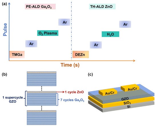
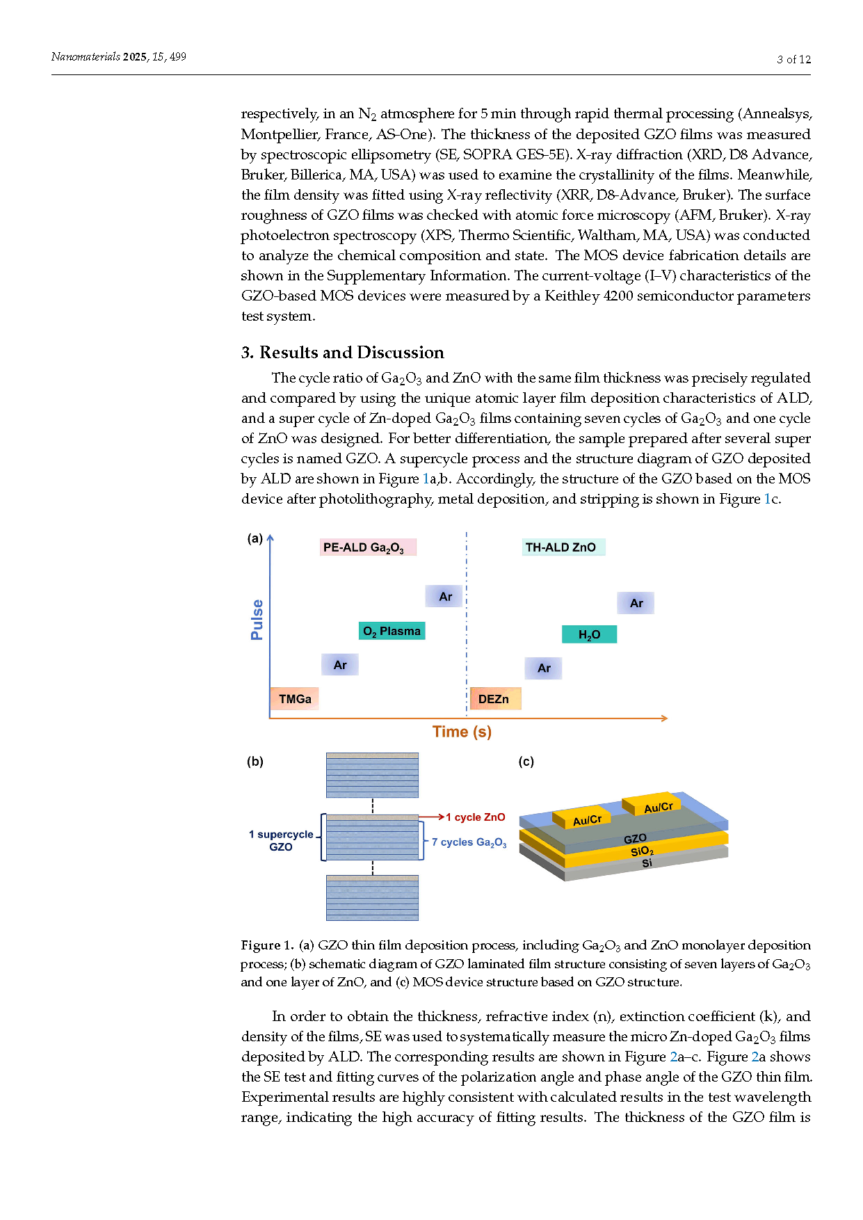
Figure 1. (a) GZO thin film deposition process, including Ga2O3 and ZnO monolayer deposition process; (b) schematic diagram of GZO laminated film structure consisting of seven layers of Ga2O3 and one layer of ZnO, and (c) MOS device structure based on GZO structure.
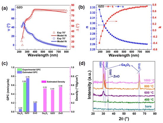
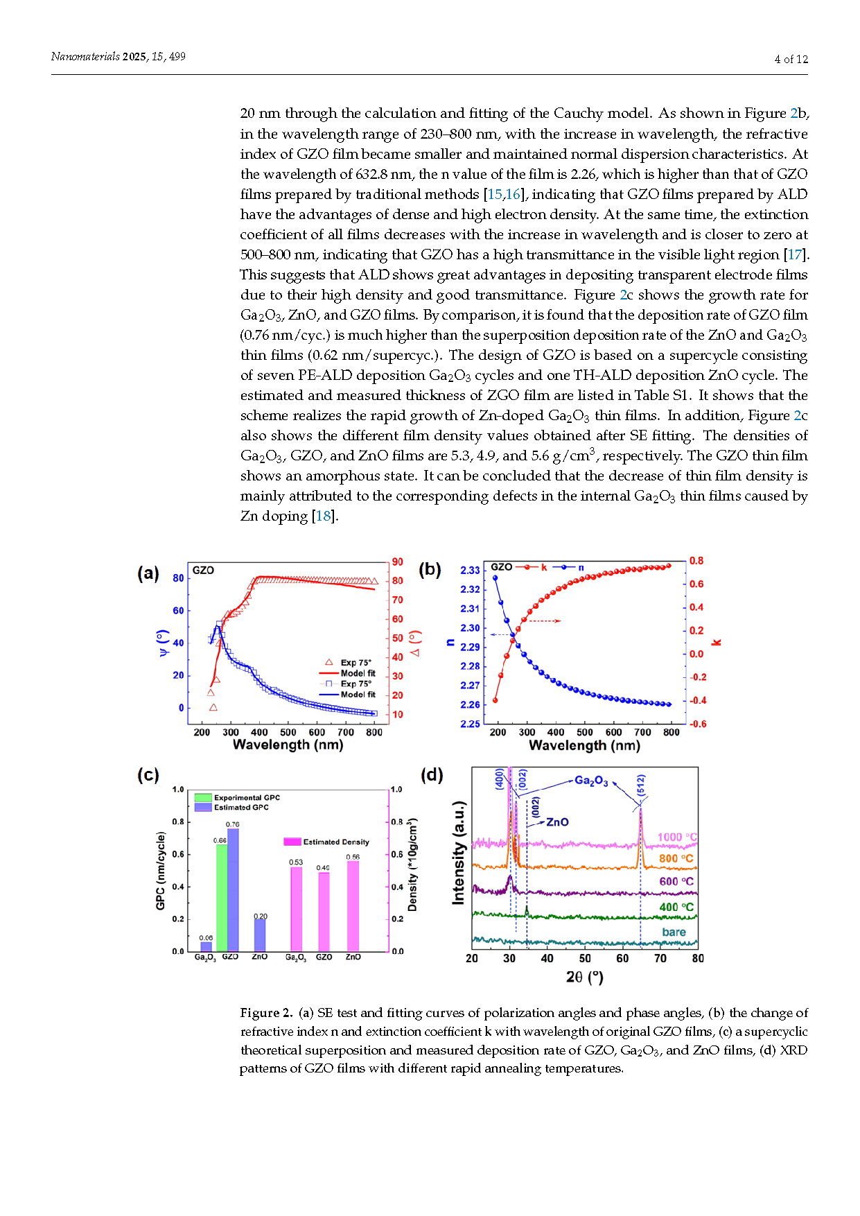
Figure 2. (a) SE test and fitting curves of polarization angles and phase angles, (b) the change of refractive index n and extinction coefficient k with wavelength of original GZO films, (c) a supercyclic theoretical superposition and measured deposition rate of GZO, Ga2O3, and ZnO films, (d) XRD patterns of GZO films with different rapid annealing temperatures.
DOI:
doi.org/10.3390/nano15070499