Paper Sharing
【International Papers】High breakdown voltage normally off Ga₂O₃ transistors on silicon substrates using GaN buffer
日期:2025-05-20阅读:760
Researchers from the King Abdullah University of Science and Technology (KAUST) have published a dissertation titled "High breakdown voltage normally off Ga2O3 transistors on silicon substrates using GaN buffer" in Applied Physics Letters.
Background
Beta gallium oxide (β-Ga2O3) has emerged as a leading ultrawide bandgap (UWBG) semiconductor material with a bandgap of approximately 4.9 eV, significantly higher than other WBG materials such as silicon carbide (SiC) and gallium nitride (GaN). This large bandgap allows Ga2O3 to sustain a critical breakdown field of up to ~8 MV cm-1, enabling its use in applications that require highvoltage and high-power capabilities. Furthermore, Ga2O3 exhibits a high Baliga’s figure of merit, which is a key indicator of power semiconductor performance. These properties make Ga2O3 a promising candidate for a wide range of high-power and high-frequency applications, including power electronics, radio frequency (RF) devices, and solar-blind ultraviolet photodetectors. Despite its advantages, several challenges hinder the widespread use of Ga2O3 in commercial applications. These include its intrinsically low thermal conductivity, which limits the device’s ability to manage heat during high-power operation, and the difficulty of achieving efficient p-type doping, which is essential for fabricating complementary devices like bipolar junction transistors.
Abstract
Normally off beta-phase gallium oxide (β-Ga2O3) metal-oxide field-effect transistors (MOSFETs) on GaN-on-Si substrates were fabricated with a threshold voltage (VTH) of 3 V. β-Ga2O3 thin films were deposited using pulsed laser deposition. The device demonstrated an excellent breakdown voltage of ∼540 V at VGS = 0 V and an extremely low gate leakage current of ∼10−7 mA/mm. Additionally, it exhibited a low subthreshold swing (SS) of ∼167 mV/dec and a current on/off ratio of ∼106. The growth and fabrication of β-Ga2O3 MOSFETs on GaN-on-Si substrates are significant for high performance and their monolithic integration with GaN devices in future power-integrated circuits.
Summary
In summary, we have effectively exhibited E-mode β-Ga2O3 MOSFETs on GaN buffer layers on Si substrates using PLD growth. The β-Ga2O3 MOSFETs have a threshold voltage of 3 V with a high breakdown voltage of ∼540 V at VGS = 0 V. The devices also showed a low subthreshold swing of ∼167 mV/dec with a low gate leakage current of ∼10−7 mA/mm in the forward bias operation of the transistors. These results highlight the significant potential of β-Ga2O3 MOSFETs for high-performance applications, demonstrating that economical and scalable PLD growth of β-Ga2O3 thin films on low-cost, commercially available GaN-on-Si substrates can be a promising route for the integration of GaN-based devices in future power and RF electronics.
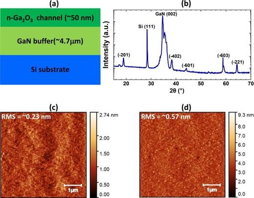
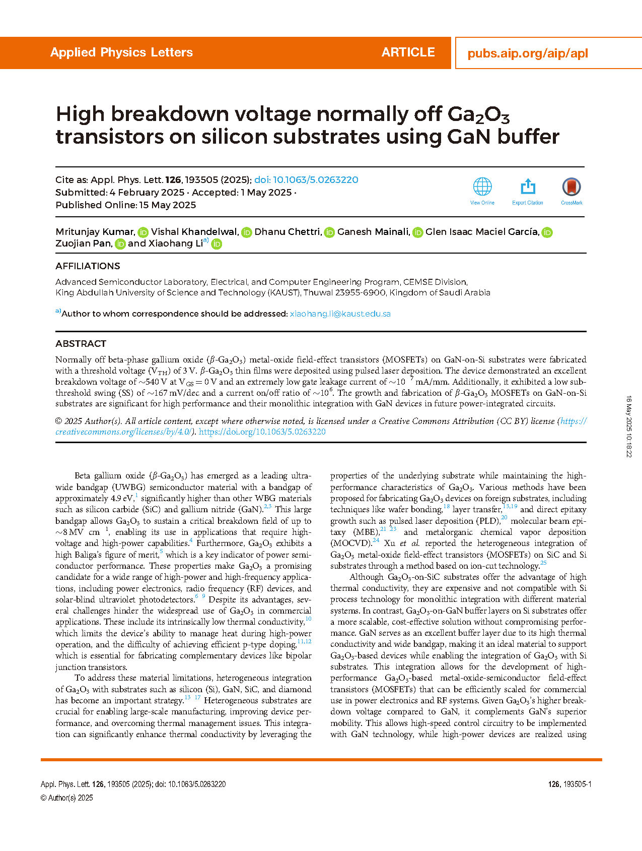
FIG. 1. β-Ga2O3 film grown on GaN-on-Si substrates: (a) schematic representation of epitaxy information, (b) XRD pattern of β-Ga2O3/GaN/Si, (c) AFM image (of 5 × 5 μm2) of GaN surface before β-Ga2O3 film deposition, (d) AFM image (of 5 × 5 μm2) after β-Ga2O3 film deposition by PLD.
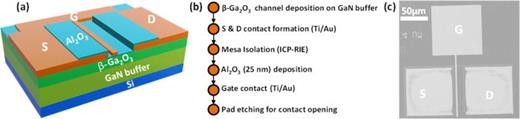
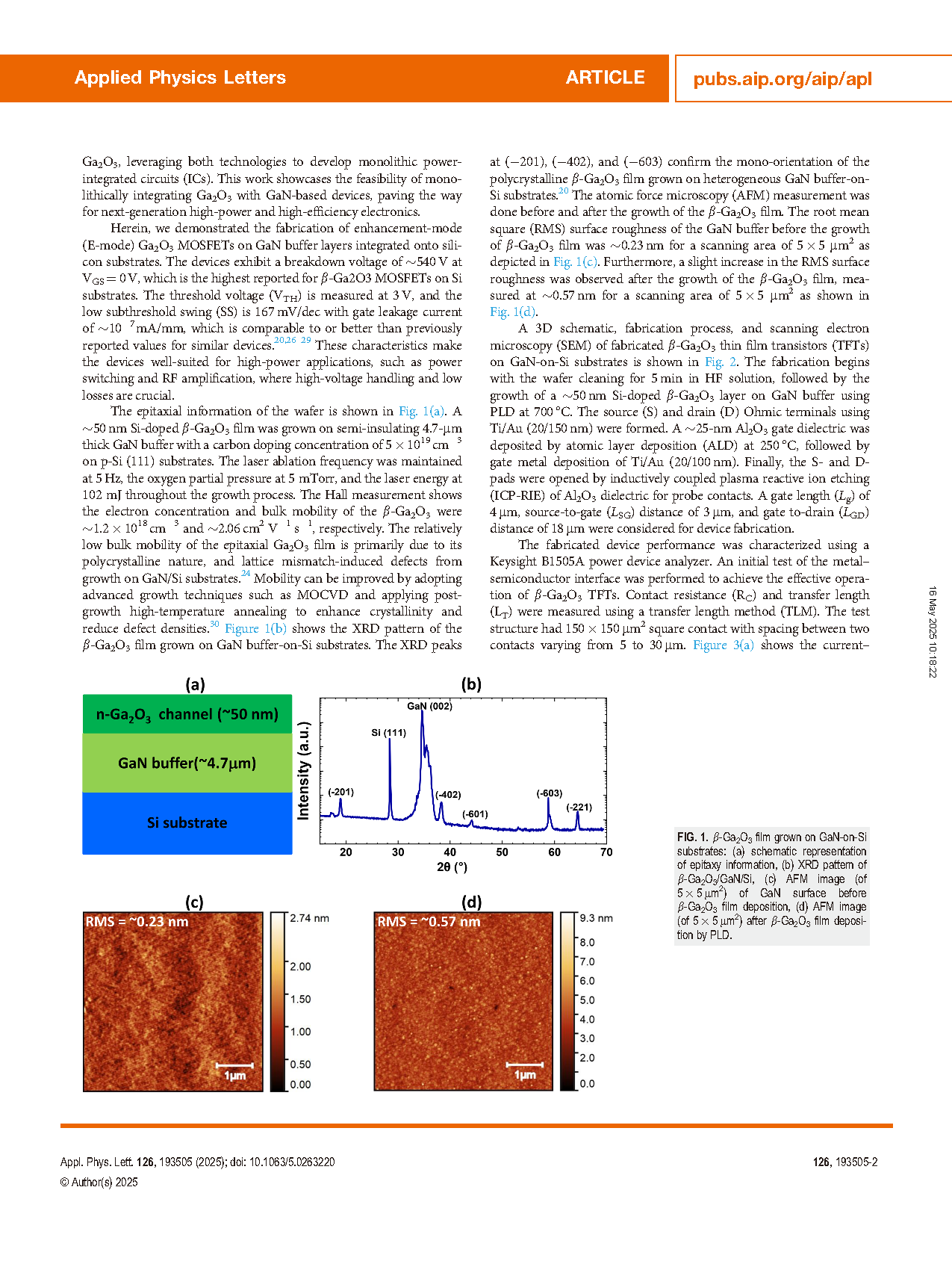
FIG. 2. The device structure of fabricated β-Ga2O3 TFTs: (a) 3D schematic, (b) process flow, (c) SEM image of the device.
DOI:
doi.org/10.1063/5.0263220