Paper Sharing
【Member Papers】Fudan University---Over 1.2 GW/cm² β-Ga₂O₃ SBD with Vbr of 1.93 kV realized by O₂ plasma and annealing
日期:2025-05-22阅读:699
Researchers from the Fudan University have published a dissertation titled "Over 1.2 GW/cm2 β-Ga2O3 SBD with Vbr of 1.93 kV realized by O2 plasma and annealing" in Semiconductor Science and Technology.
Project Support
This work was supported by Shanghai Municipal Science and Technology Commission under Grant 23511102300 and 24DP1500105.
Background
In this study, the electrical performance of β-Ga2O3 Schottky barrier diode (SBD) has been significantly enhanced through the application of O2 plasma and annealing treatment (OPAT). Compared to the control device, the OPAT β-Ga2O3 SBD exhibits superior turn-on voltage (Von), specific on-resistance (Ron,sp) and breakdown voltage (Vbr).
Abstract
In this study, the electrical performance of β-Ga2O3 Schottky barrier diode (SBD) has been significantly enhanced through the application of O2 plasma and annealing treatment (OPAT). Compared to the control device, the OPAT β-Ga2O3 SBD exhibits superior turn-on voltage(Von), specific on-resistance (Ron,sp) and breakdown voltage (Vbr). Moreover, by incorporating electron-beam evaporated Al2O3 as the field plate oxide, the surface breakdown electric field increases from 2.19 MV/cm to 4.09 MV/cm, as extracted by TCAD simulation. The OPAT field-plated β-Ga2O3 SBD achieves Von of 0.52 V at the current density of 1 A/cm2, Ron,sp of 3.10 mΩ·cm2, and Vbr of 1.93 kV. Its power figure of merit reaches 1.2 GW/cm2. X-Ray Photoelectron Spectroscopy measurements indicate that OPAT reduces the concentration of oxygen vacancy, which in turn decreases the Schottky barrier height of the device, consequently enhancing the performance of β-Ga2O3 SBD. These results demonstrate the enormous potential of β-Ga2O3 in low Von and high Vbr applications.
Conclusion
In summary, we have investigated the effects of OPT and OPAT on the performance of β-Ga2O3 SBDs. XPS measurement indicates that the relative percentage of the VOs significantly decreases by OPAT. TCAD simulation suggests that the surface electric field of the OPAT FP sample is almost twice that of the control sample. The OPAT FP device accomplishes Von of 0.52 V, Ron,sp of 3.10 mΩ·cm2 , and Vbr of 1.93 kV. It maintains a low Von while reaching a PFOM of 1.2 GW/cm2. These results demonstrate that the OPAT and FP structure fabricated by EBE are highly promising for boosting the performance of β-Ga2O3 SBDs in power electronics.
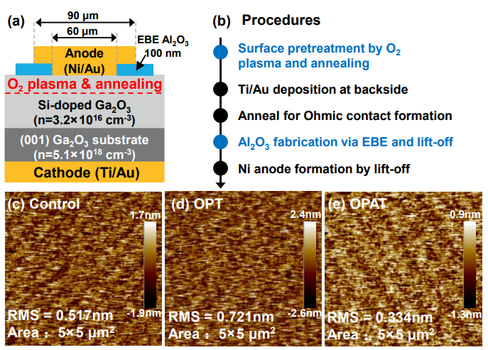
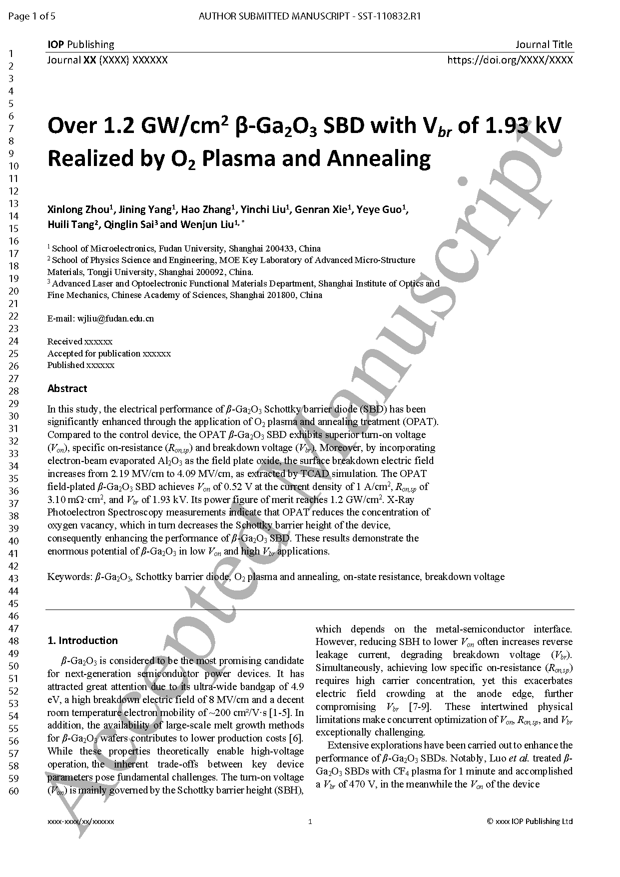
Fig. 1. (a) Schematic and (b)fabrication procedure of the OPAT FP β-Ga2O3 SBD. Surface morphology of the (c) control, (d) OPT, (e) OPAT sample measured by AFM.
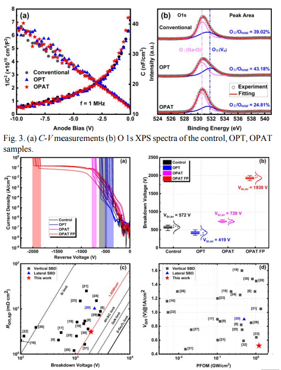
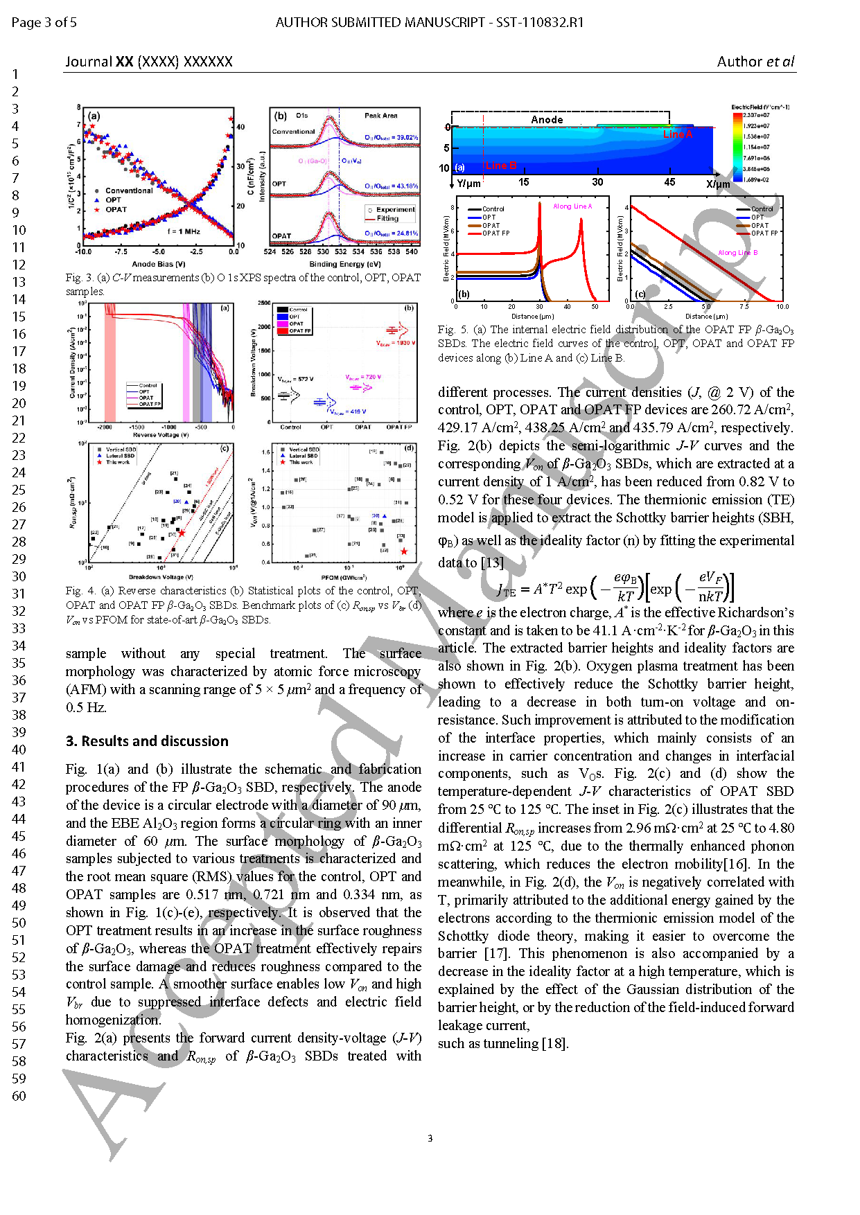
Fig. 2. (a) Reverse characteristics (b) Statistical plots of the control, OPT, OPAT and OPAT FP β-Ga2O3 SBDs. Benchmark plots of (c) Ron,sp vs Vbr (d) Von vs PFOM for state-of-art β-Ga2O3 SBDs.
DOI:
doi.org/10.1088/1361-6641/adcd24