Paper Sharing
【Domestic Papers】University of Science and Technology Beijing --- Ultrasensitive Deep-Ultraviolet Photodetectors Based On Band Engineering and Ferroelectric Modulation
日期:2025-05-22阅读:860
Researchers from the University of Science and Technology Beijing have published a dissertation titled "Ultrasensitive Deep-Ultraviolet Photodetectors Based On Band Engineering and Ferroelectric Modulation" in Advanced Materials.
Project Support
H.W., L.S., and Q.Z. contributed equally to this work. This research was supported by the National Key R&D Program of China (2020YFA0406202), the National Natural Science Foundation of China (22090042, 21971009, and 62204125), Guangxi BaGui Scholars Special Funding, and the Fundamental Research Funds for the Central Universities, China (FRF-IDRYGD21-03 and GJRC003). The authors gratefully acknowledge the cooperation of the beamline scientists at the Beijing Synchrotron Radiation Facility 1W1A beamline. The noise spectrum density was measured by the low-frequency noise test system (LFN-2000), Wuxi Xinjian semiconductor Tech Co,.Ltd.
Background
Deep-ultraviolet (DUV) photodetectors (PDs) are essential in various fields such as UV imaging, environmental monitoring, military defense, and biological detection. Several wide-bandgap semiconductors, including AlN, ZnO, GaN, and Ga2O3, have garnered significant attention for DUV photodetectors. Among these, Ga2O3 is a desired candidate on accounts of its suitable direct bandgap of approximately 4.9 eV, high breakdown electric field of around 8 MV cm−1, high absorption coefficient, and thermal stability…
Abstract
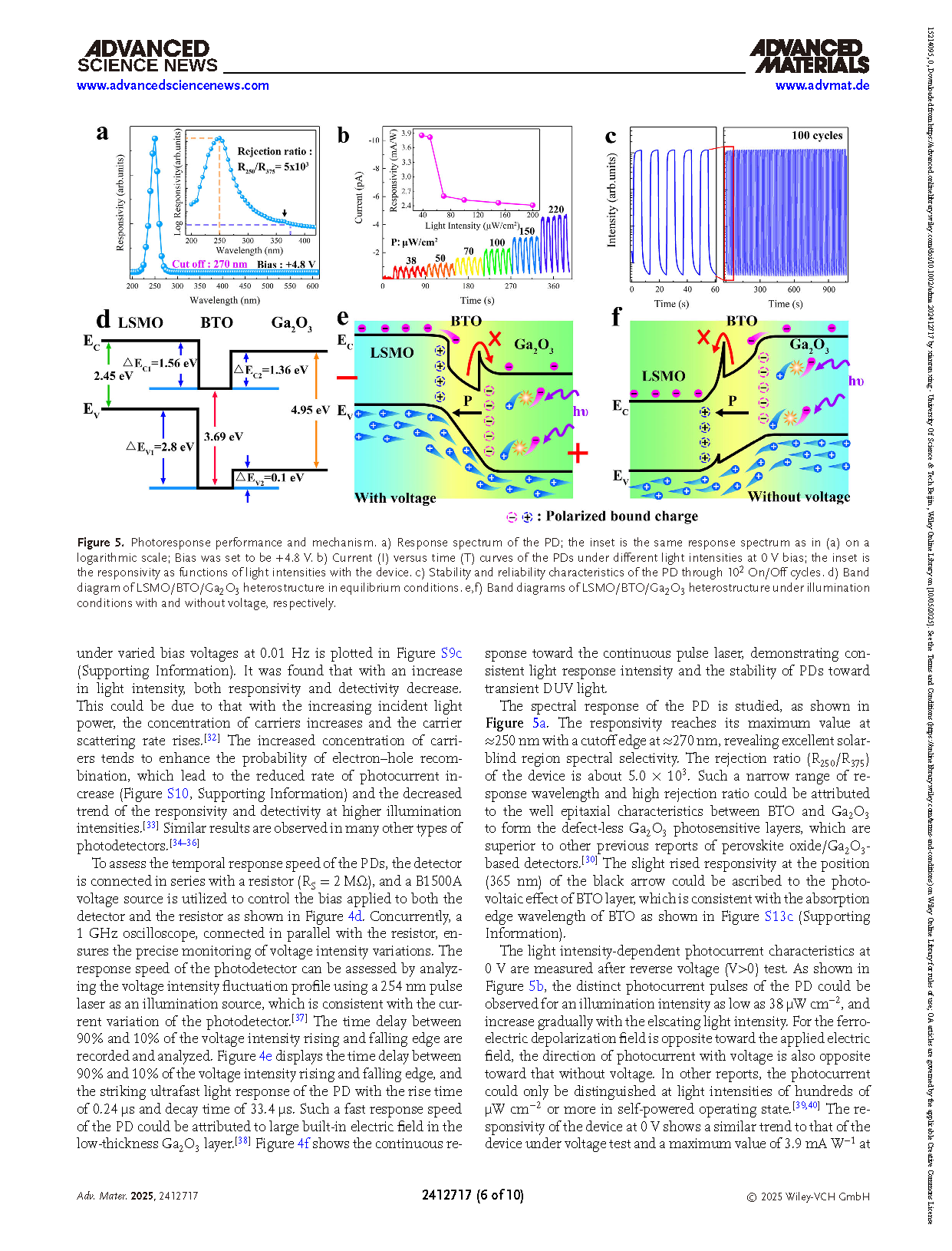
Wide bandgap semiconductors have emerged as a class of deep-ultraviolet sensitive materials, showing great potentials for next-generation integrated devices. Yet, to achieve a high photoresponse of deep-ultraviolet detector without complicated designs at low supply voltage and weak light intensity is challenging. Herein, a new way is designed to fabricate an ultrasensitive vertical-structured photodetector with epitaxial 7 nm BaTiO3 interlayer and 10 nm Ga2O3 photosensitive layer, realizing the detection to a rare weak deep UV light intensity (0.1 µW cm−2) at a voltage under 4.8 V and demonstrating a surge in responsivity up to 1.1 A W−1 with ultrafast response of 0.24 µs/33.4 µs (rise/decay). A responsivity of 3.8 mA W−1 at 0 V also has been reached. The dark current is suppressed by enlarged conduction band offset and meanwhile the photocurrent is enhanced by unidirectional conducting valance band offset, which formed by BaTiO3 interlayer. BaTiO3 also contributes most to the photoresponse at 0 V through its ferroelectric depolarization electric field. These results provide a path toward high-sensitive, low-power-consumption, and highly-integrated deep-ultraviolet detection, beyond conventional ones.
Conclusion
In summary, we present an ultrasensitive vertical-structured DUV PDs integrated with epitaxial ultrathin BaTiO3 interlayers and Ga2O3 photosensitive layers, meeting the needs of high response, low supply voltage, and highly integrated characteristics in future advanced semiconductor industry. The PD shows high performance with a responsivity value of 1.1 A W−1 at 4.8 V and 0.1 μW cm−2, 38 mA W−1 at 0 V and 38 μW cm−2, and ultrafast response of 0.24 μs/33.4 μs (rise/decay). Fine manipulation of energy band and the effect of ferroelectric depolarization electric field realizes such a high photoresponse performance. Hence, this type of DUV PD combined with the integrating compatibility with CMOS in this work offers a promising materials design platform to build future high-sensitive and low-power-consumption Ga2O3-based electronic and optoelectronic devices.
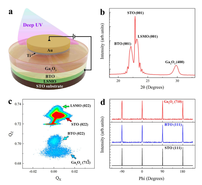
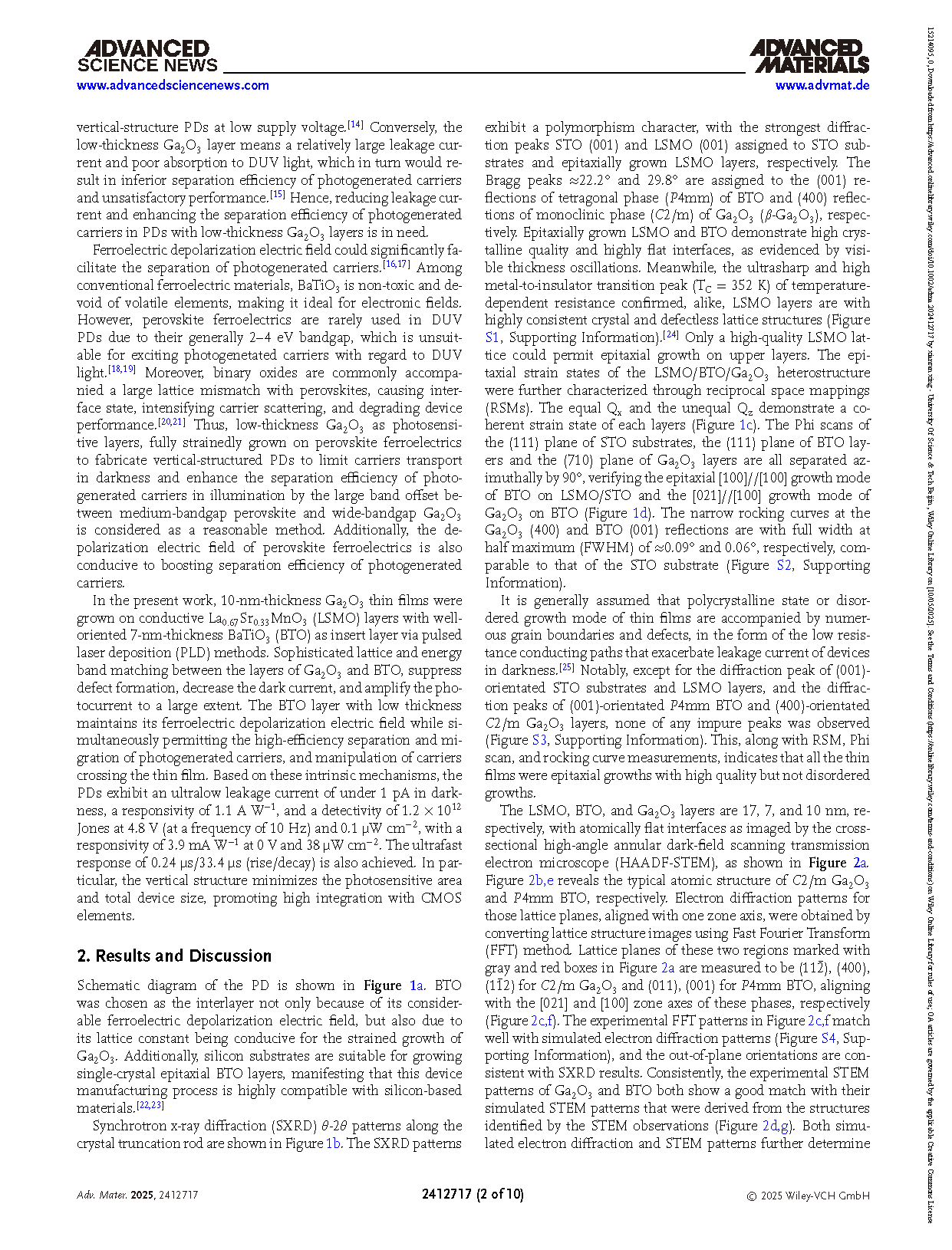
Figure 1. Schematic and structural characterization of LSMO/BTO/Ga2O3 heterostructure. a) Schematic view of the PD. b) Synchrotron-based XRD pattern of the sample in (a). c) X-ray reciprocal space mapping (RSM) images around the STO (022) reflection for the LSMO/BTO/Ga2O3 heterostructure. d) The Phi scans of the (710), (111), and (111) planes of Ga2O3, BTO, and STO, respectively.
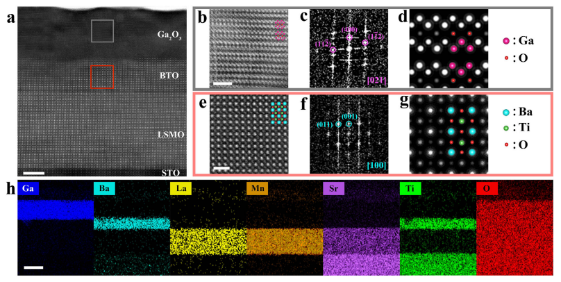
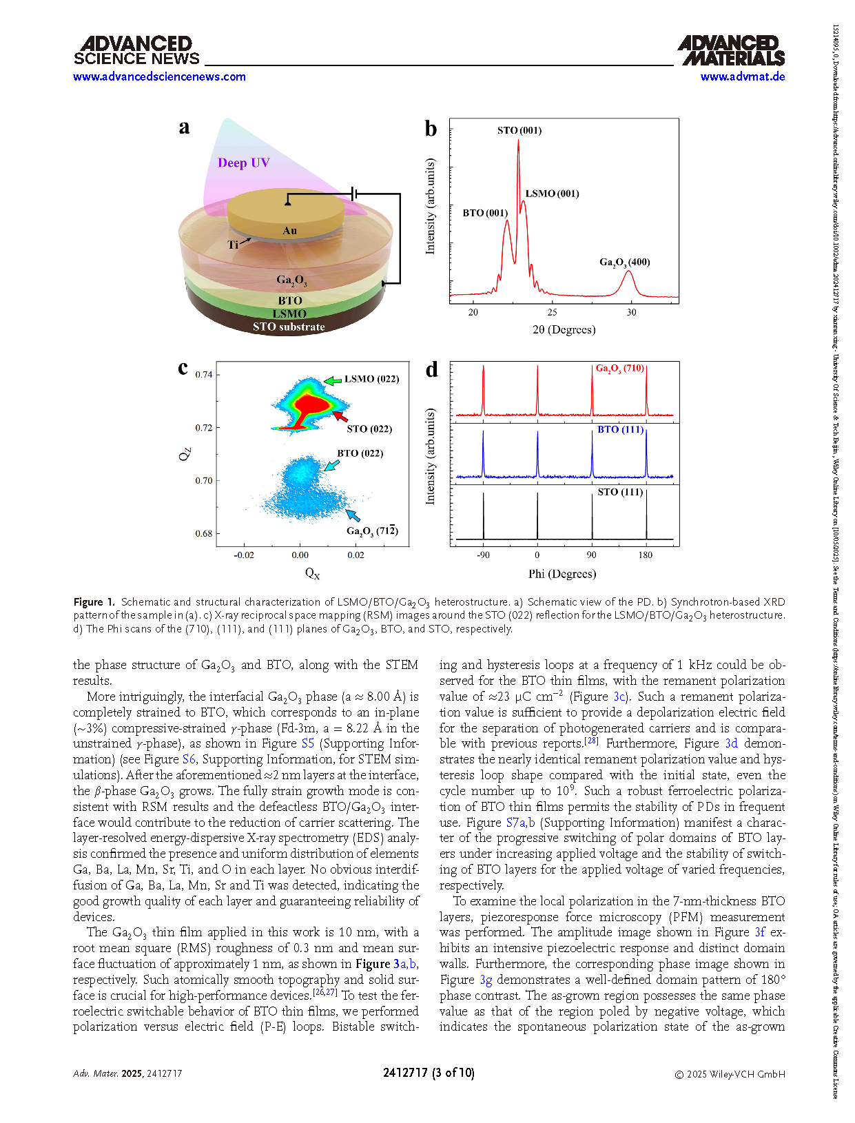
Figure 2. Atomic-resolution STEM analysis of LSMO/BTO/Ga2O3 heterostructure. a) Representative cross-sectional HAADF-STEM image of the LSMO/BTO/Ga2O3 heterostructure. Scale bar, 5 nm. b,e) Enlarged atomic structure images for the regions marked with gray and red boxes in (a), respectively. Scale bar, both 1 nm. The image of (b) was filtered with the IFFT method. c, f) The corresponding FFT patterns of the regions marked with gray and red boxes in (a). d,g) Simulated STEM images corresponding to the experimental STEM images for Ga2O3 and BTO, respectively. The Ga, Ba, Ti and O lattice models used for the experimental and simulated STEM images were overlaid on each image for comparison. h) Corresponding EDS mapping showed the distribution of Ga, Ba, La, Mn, Sr, Ti, and O. Scale bar, 10 nm.
DOI:
doi.org/10.1002/adma.202412717