


Member News
【Member News】Shenzhen Pinghu Laboratory Independently Develops Integrated Characterization System of Ultra-Wide Bandgap Semiconductor Materials and Devices
日期:2025-05-23阅读:884
As the physical operation unit of the National Center of Technology Innovation for Wide Bandgap Semiconductor (Shenzhen), the Shenzhen Pinghu Laboratory's Fourth Generation Semiconductor Materials and Devices Research Group focuses on the fields of diamond, Aluminum Nitride and Gallium Oxide materials and devices, and is committed to developing advanced growth technologies for fourth generation semiconductor materials, device fabrication processes and heterogeneous integration. Promote the application of relevant materials and devices in multiple fields such as smart grids, power electronics, aerospace, new energy, optoelectronics and special environments. At present, specialized laboratories for theoretical simulation, material growth, device design and fabrication, and performance testing have been established in the direction of fourth-generation semiconductor research.
The core equipment currently available in this laboratory includes Metal-Organic Chemical Vapor Deposition (MOCVD), Molecular Beam Epitaxy (MBE), Electron Beam Lithography (EBL), Inductively Coupled Plasma Reactive Ion Etching (ICP-RIE), Magnetron Sputtering machines, Plasma-Enhanced Chemical Vapor Deposition (PECVD), and other equipment required for the growth of epitaxial materials, device fabrication, and measurement. Given that there is no commercial characterization system for 6.2eV ultra-wide band gap semiconductor materials and ultra-high voltage high-power devices in the industry at present, the laboratory independently designed the first multi-functional ultra-wide band gap material and 10,000-volt high-power device Integrated characterization system in domestic and international, successfully filling the gap in this field.
The ultra-wide band gap material characterization section (Figure 1) includes a deep ultraviolet excitation light source, a spectrophotometer, a vacuum system, an adjustable temperature platform, a deep ultraviolet microscope, a multifunctional bidirectional detector, a DC power supply, etc. It can measure the optical bandgap, minority carrier lifetime, and electrical conductivity of ultra-wide band gap semiconductors including aluminum nitride within the required temperature range. It can also measure in situ the material parameters and changes before and after bias and under bias conditions.
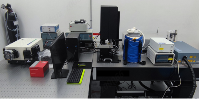
Figure 1. Integrated Characterization System: Material Characterization Section
The device characterization section of the integrated characterization system (Figure 2) includes a high withstand voltage and high temperature resistance test platform, a high vacuum system, a temperature control system, a 12kV/1A adjustable high-voltage power supply, a 50A/3000V high-power power supply, and a 0-50V adjustable low-voltage power supply, etc. The output characteristics and forward/reverse characteristics of different types of high-voltage and high-power devices can be measured within the desired temperature range. The system is also equipped with fiber optic detectors of different bands and window measurement devices to emit defect light under the condition of bias voltage. This system is currently the only multi-functional integrated characterization system capable of characterizing ultra-wide band gap semiconductor materials including aluminum nitride and high withstand voltage and high-temperature resistant power devices, and has been authorized by the Patent Office of the National Intellectual Property Administration.
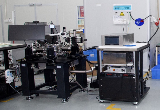
Figure 2. Integrated Characterization System: Device Characterization Section
The design and development of this system will undoubtedly provide significant support for the research of ultra-wide band gap semiconductor materials and devices, and also demonstrate the forward-looking layout and scientific research strength of Shenzhen Pinghu Laboratory in this scientific research field.
