Paper Sharing
【Domestic Papers】Shandong University---Edge-Dependent Step-Flow Growth Mechanism in β-Ga₂O₃ (100) Facet at the Atomic Level
日期:2025-05-29阅读:1097
Researchers from the Shandong University have published a dissertation titled "Edge-Dependent Step-Flow Growth Mechanism in β-Ga2O3 (100) Facet at the Atomic Level" in The Journal of Physical Chemistry Letters
Project Support
This work was supported by the National Natural Science Foundation of China (Grants 5193000206, U24A20312, 62374079, and 62304097), National Key Research and Development Plan (Grants 2024YFA1208802 and 2023YFB4606900), Guangdong Basic and Applied Basic Research Foundation (Grants 2023A1515012048 and 2024A1515030224), and Shenzhen Fundamental Research Program (Grants JCYJ20230807093609019, JCYJ20220530114615035, JCYJ20240807170626004, and 2023112115707001). The computational resources are provided by the Center for Computational Science and Engineering at the Southern University of Science and Technology.
Background
Gallium oxide (Ga2O3) has garnered enormous interest from the (opto-)electronics community as a promising next-generation ultrawide bandgap semiconductor. Among its polymorphs, the monoclinic β-Ga2O3, the most stable phase under ambient conditions, exhibits several remarkable properties, including an ultrawide bandgap (Eg ≃ 4.9 eV), a high breakdown electric field (Ecrit ≃ 8 MV/cm), exceptional chemical and thermal stability (melting point ≃ 1720 °C), a large Baliga’s figure of merit (BFOM = 3444), a short ultraviolet cutoff edge of ∼ 260 nm, and high radiation resistance. Owing to these outstanding material properties, β-Ga2O3 possesses great prospects for applications in high-power electronics, solar-blind ultraviolet optoelectronics, and two-dimensional devices. To fabricate a high-performance β-Ga2O3-based device, a high-quality epitaxial thin film with a smooth surface and low defect density is essential. Particularly, homoepitaxy is significant for minimizing defect density in the β-Ga2O3 epitaxial thin film by avoiding lattice mismatch in heteroepitaxy. Recently, the homoepitaxy of β-Ga2O3 has been explored using several thin film growth techniques, such as metal−organic vapor phase epitaxy (MOVPE) (also referred to as metal−organic chemical vapor deposition, MOCVD, in the literature, molecular beam epitaxy (MBE), halide vapor phase epitaxy (HVPE), and mist chemical vapor deposition (mist-CVD).
Abstract
Homoepitaxial step-flow growth of high-quality β-Ga2O3 thin films is essential for the advancement of high-performance Ga2O3-based devices. In this work, the step-flow growth mechanism of the β-Ga2O3 (100) facet is explored by machine-learning molecular dynamics simulations and density functional theory calculations. Our results reveal that Ga adatoms and Ga–O adatom pairs, with their high mobility, are the primary atomic species responsible for efficient surface migration on the (100) facet. The asymmetric monoclinic structure of β-Ga2O3 induces a distinct two-stage Ehrlich–Schwoebel barrier for Ga adatoms at the [00−1] step edge, contributing to the suppression of double-step and hillock formation. Furthermore, a miscut toward [00−1] does not induce the nucleation of stable twin boundaries, whereas a miscut toward [001] leads to the spontaneous formation of twin boundaries. This research provides meaningful insights not only for high-quality β-Ga2O3 homoepitaxy but also the step-flow growth mechanism of other similar systems.
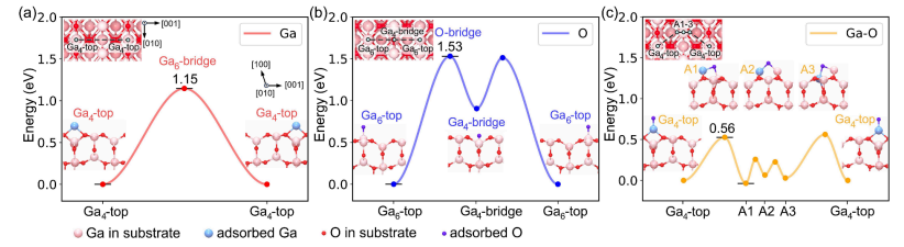
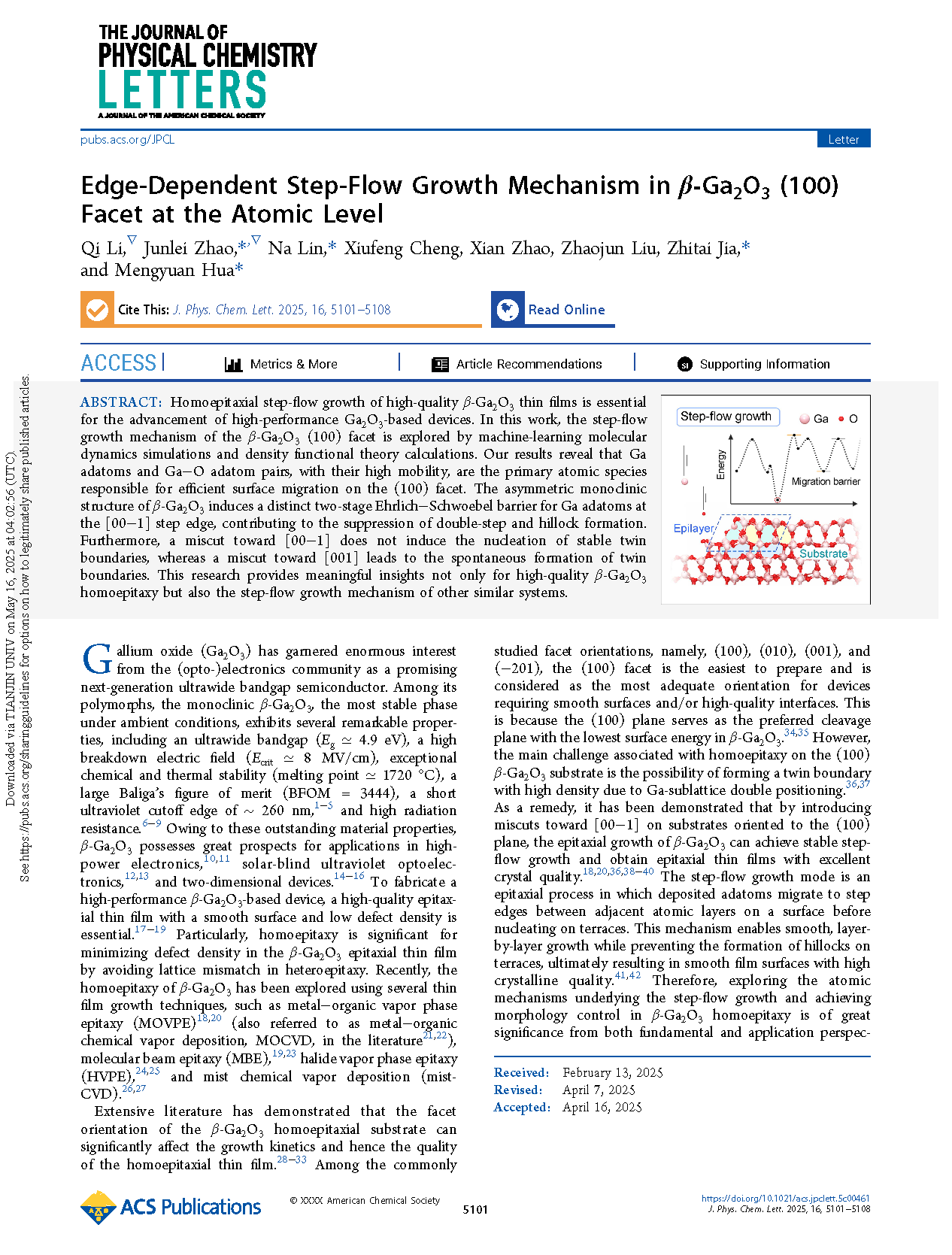
Figure 1. MEBs for (a) a Ga adatom (big lightblue sphere), (b) an O adatom (small purple sphere), and (c) a Ga−O adatom pair on the (100) surface of β-Ga2O3. Substrate Ga and O atoms are shown in pink and red, respectively. Insets at the top-left corners of the three panels provide the top views of the corresponding MEPs. The curves represent the fitted MEBs, with each valley point corresponding to the adjacent structure. Ga4 and Ga6 denote the four-coordinated and six-coordinated Ga substrate sites, respectively.
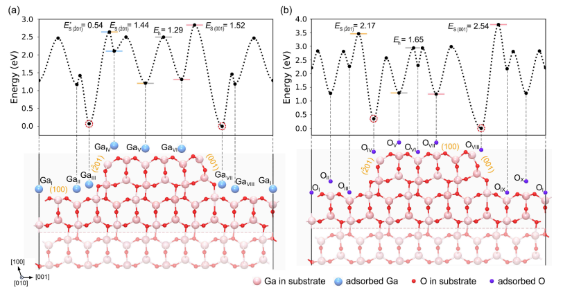
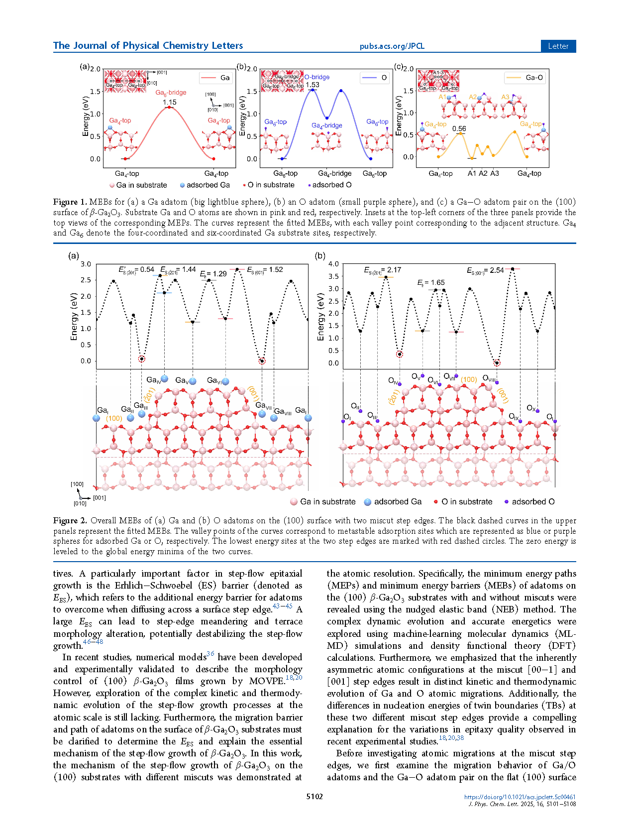
Figure 2. Overall MEBs of (a) Ga and (b) O adatoms on the (100) surface with two miscut step edges. The black dashed curves in the upper panels represent the fitted MEBs. The valley points of the curves correspond to metastable adsorption sites which are represented as blue or purple spheres for adsorbed Ga or O, respectively. The lowest energy sites at the two step edges are marked with red dashed circles. The zero energy is leveled to the global energy minima of the two curves.
DOI:
doi.org/10.1021/acs.jpclett.5c00461