Paper Sharing
【Member Papers】Xidian University---Preliminary development and high-voltage lifetime testing of vertical photoconductive semiconductor switches based on Fe-doped β-Ga₂O₃
日期:2025-05-30阅读:1041
Researchers from the Xidian University have published a dissertation titled " Preliminary development and high-voltage lifetime testing of vertical photoconductive semiconductor switches based on Fe-doped β-Ga2O3" in High Power Laser and Particle Beams.
Background
Optical switch is one of the high-performance high-power switches currently available, which can quickly switch between high resistance and conduction states under the action of light. Compared to traditional switches, optical switches have many advantages such as minimal turn off time and time jitter, resistance to electromagnetic interference, lightweight, and small size The size of the bandgap width of the material will affect the suitable input laser pulse wavelength and the temperature range of the device operation for the optical switch. Generally, materials with larger bandgap widths work more stably at high temperatures and high currents, and are more suitable for preparing high-power devices. The development history of optical switches can be traced back to the 1970s. In 1972, S. Jayaraman et al. from the University of Maryland, Park, USA, studied the optical properties of gallium arsenide and found that its light response frequency was very close to the laser frequency. They concluded that the light response time of some semiconductor materials was in the ps range In 1975, D. H. Auston et al. from Bell Laboratories in the United States observed the effect of single crystal silicon on 532 nm and1064 nm wavelength laser can generate ps level response In 1976, P. Lefur and D. H. Auston prepared the world's first semiconductor optical switch based on single crystal Si Subsequently, research on optical switches has become increasingly vigorous. There is also some research in the field of optical switches in China. In 2008, Yan Chengfeng and others from the Chinese Academy of Sciences Shanghai Institute of Silicate developed the first semi insulated 6H SiC photoconductive switch in China, with a rise time of 6.8 ns Subsequently, a group of universities and institutions have also started exploring related fields. However, there is still limited research on gallium oxide based optical switches both domestically and internationally. K. M. Dowling and others from the Department of Microelectronics at Delft University of Technology in the Netherlands were among the first to produce and demonstrate β - Ga2O3PCSS, They tested the carrier lifetime and DC characteristics of the planar switch, indicating that Fe: β - Ga2O3Having high breakdown field strength and moderate photoelectric response characteristics, although the light dark current is relatively low under specific conditions, it still verifies Fe: β - Ga2O3The potential of PCSS materials as harsh environmental applications.
Abstract
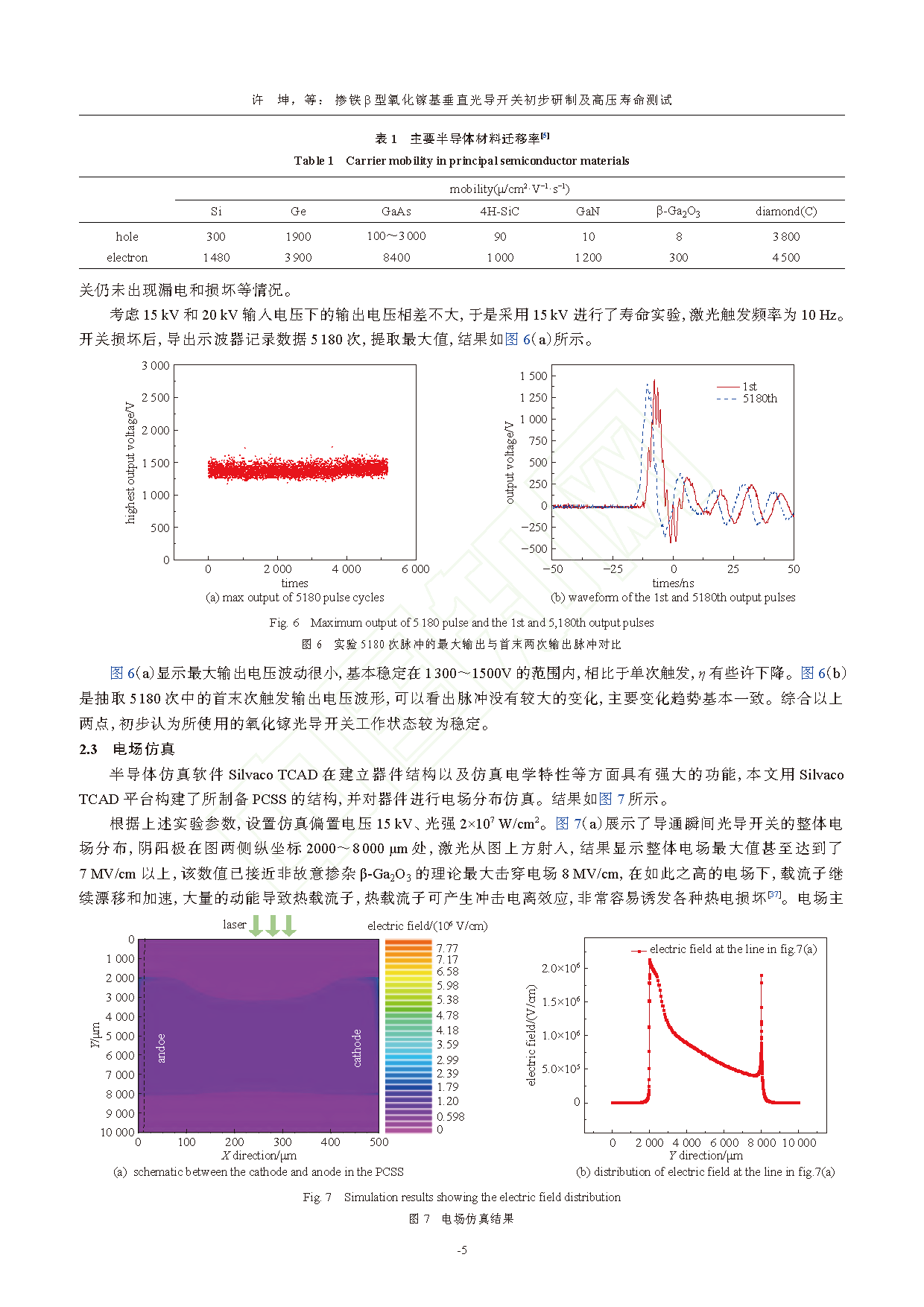
This study focuses on the performance of vertical photoconductive semiconductor switch (PCSS) based on Fe: β-Ga2O3 under high voltage. The results show that deep levels in Fe: β-Ga2O3 can provide carriers of non-intrinsic excitation. The device did not exhibit breakdown tendencies when subjected to a 20 kV input voltage with single-shot laser triggering. After more than 5000 trigger cycles at 15 kV by a 10 Hz laser, the switch eventually failed. Nevertheless, pulse performance remained stable throughout the effective data collection period, preliminarily demonstrating the potential of Ga2O3 PCSS for applications in extreme conditions such as high power and high frequency. Failure analysis indicates that a wide bandgap is not the sole determinant of high breakdown voltage. In addition to employing precise doping techniques to introduce specific defects and modify material properties, further improvements in existing material growth methods and device packaging structures can also contribute to enhancing the output and lifetime of PCSS.
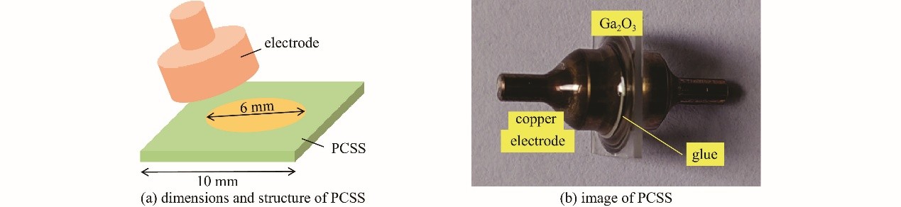
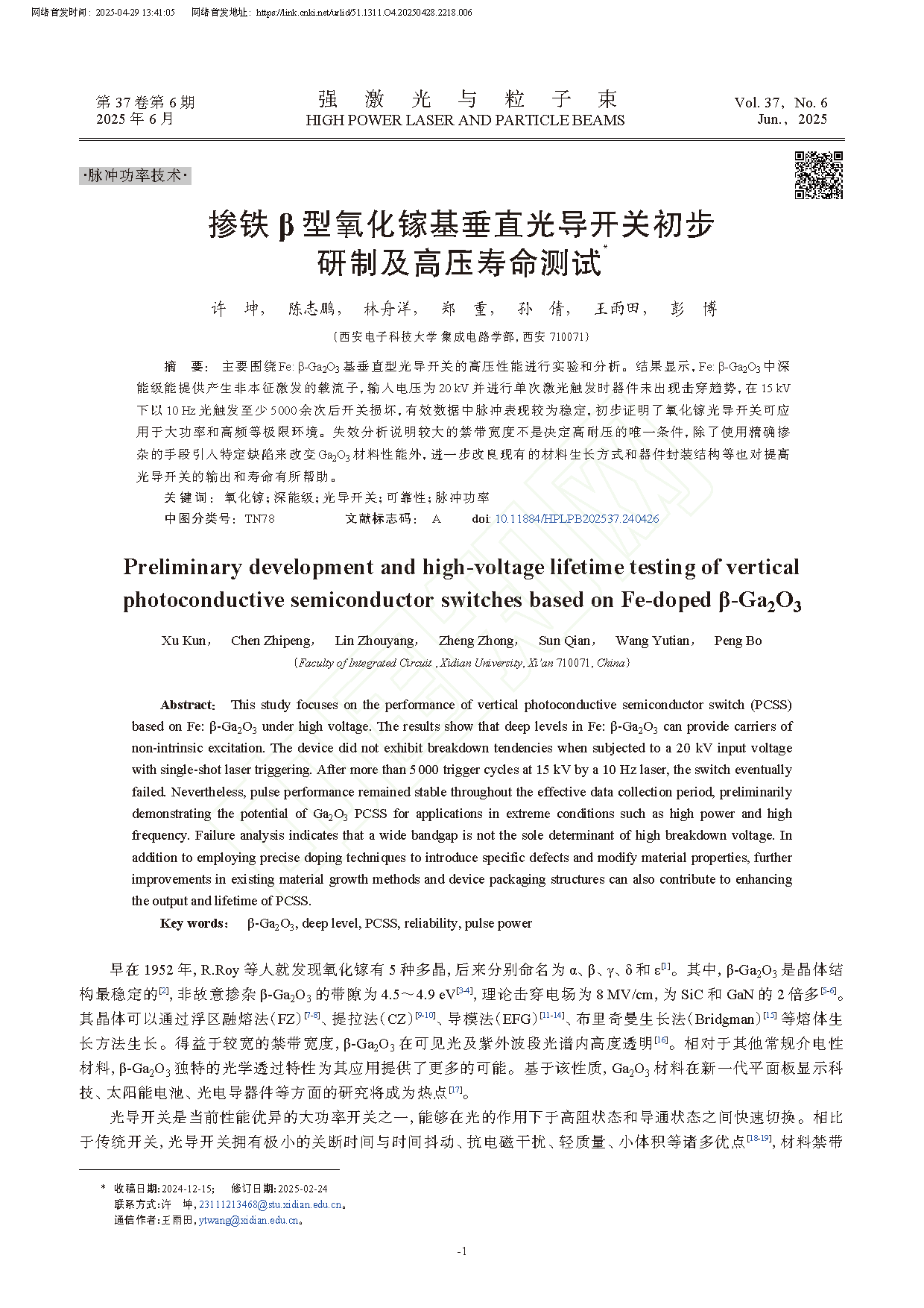
Figure 1. PCSS fabricated by encapsulating gallium oxide with copper electrodes
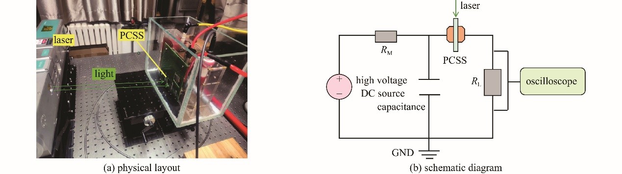
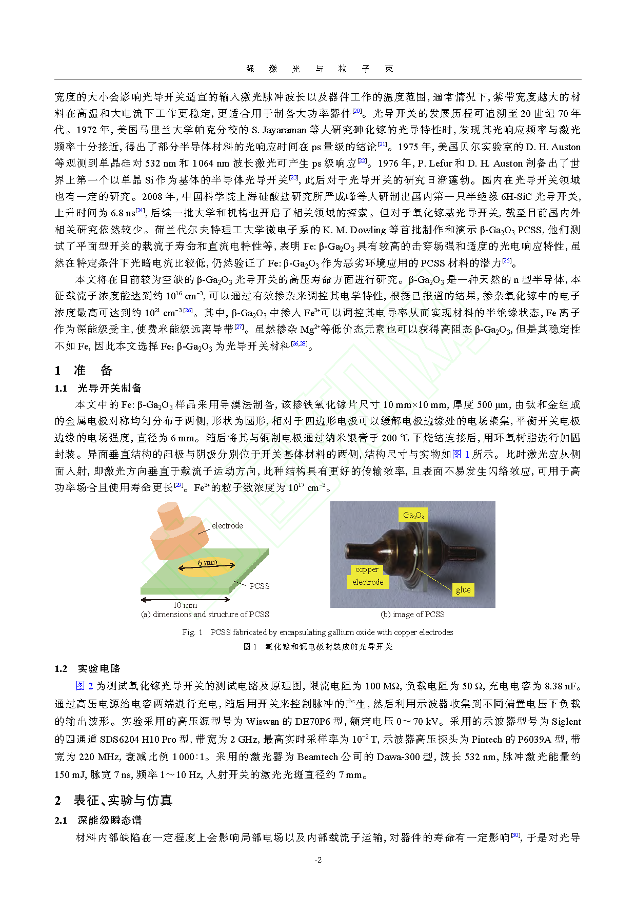
Figure 2. Diagram of test system and experimental circuit
DOI:
doi.org/10.11884/HPLPB202537.240426