Paper Sharing
【Domestic Papers】Sun Yat-Sen University --- Growth of Ga₂O₃ thin films on Si(111) substrates by metal-organic chemical vapor deposition
日期:2025-05-30阅读:1096
Researchers from the Sun Yat-Sen University have published a dissertation titled "Growth of Ga2O3 thin films on Si(111) substrates by metal-organic chemical vapor deposition" in Vacuum.
Project support
This work was supported by the Natural Science Foundation of China (Grant No. 62074167), the Research and Development Plan Project of Guangdong Province (No. 2021B0101300005).
Background
Ga2O3 is an attractive semiconductor for applications in solar-blind ultra-violet detectors, heterojunction PN diodes, Schottky barrier diodes (SBDs), and field effect transistors (FETs) due to its ultra-wide bandgap (Eg = 4.4–5.3 eV), high breakdown electric field strength (Ebr = 3.8–8 MV/cm) , and large dielectric constant (εr = 10–32) . The Ga2O3 family includes five polymorphs: α, β, γ, δ, and ε (also referred to as κ). Among these Ga2O3 polymorphs, β-Ga2O3 is the most thermodynamically stable phase, and it has been the focus of intensive investigation. However, its relatively high cost, low thermal conductivity, and anisotropy properties severely hinder the industrialization of β-Ga2O3-based applications. The other four polymorphs exhibit a tendency for thermostability in the order of ε > α > δ > γ, and they can ultimately be transformed into the β-phase structure as the annealing temperature increases. The α-Ga2O3 phase, which belongs to the trigonal corundum structure and possesses the largest bandgap (Eg = 5.3 eV), can be converted to β-Ga2O3 when the growth temperature exceeds 550 °C. The cubic bixbyite structure δ-Ga2O3, characterized by a lattice constant of 0.9225 nm, was successfully epitaxially grown on β-Fe2O3 buffer layers for the first time in 2023. Furthermore, γ-Ga2O3 is characterized by a defective cubic spinel structure with a lattice parameter of a = 0.822 nm and exhibits lower growth temperatures (<500 °C) .
Abstract
Low-cost and large-scale Ga2O3 epitaxial films are crucial for commercial applications based on Ga2O3. Traditional homoepitaxial β-Ga2O3 faces significant challenges in terms of cost-effectiveness. Therefore, the realization of heteroepitaxy of ε-Ga2O3 thin films on commercially mature silicon substrate is important. In this study, we conducted systematic investigations into the growth of Ga2O3 films on Si(111) substrates to explore the growth mechanism. Based on a comprehensive analysis of X-ray diffraction (XRD), optical microscopy (OM), scanning electron microscopy (SEM), and transmission electron microscopy (TEM), it is evident that the presence of amorphous SiOx and Ga2O3, the existence of β-nuclei, and numerous inclined Ga2O3 islands significantly degrade the crystal quality and surface morphology. Furthermore, the disordered atomic arrangement and the lack of coalescence of the epilayer can primarily be attributed to the oxidation of the silicon face, as observed through high-resolution TEM measurements. This study elucidates the evolution process of Ga2O3 nuclei and offers profound insights into the growth mechanisms during the early growth stage on the silicon substrate, which are essential for obtaining high-quality silicon-based ε-Ga2O3 films.
Highlights
• The growth investigation of Ga2O3 thin films on Si(111) substrates via MOCVD was conducted.
• The presence of amorphous SiOx on the silicon surface adversely affects the crystalline quality of Ga2O3.
• The main growth issues of silicon-based Ga2O3 arise from the amorphous layer, mixed phases, and grain distortion.
Conclusions
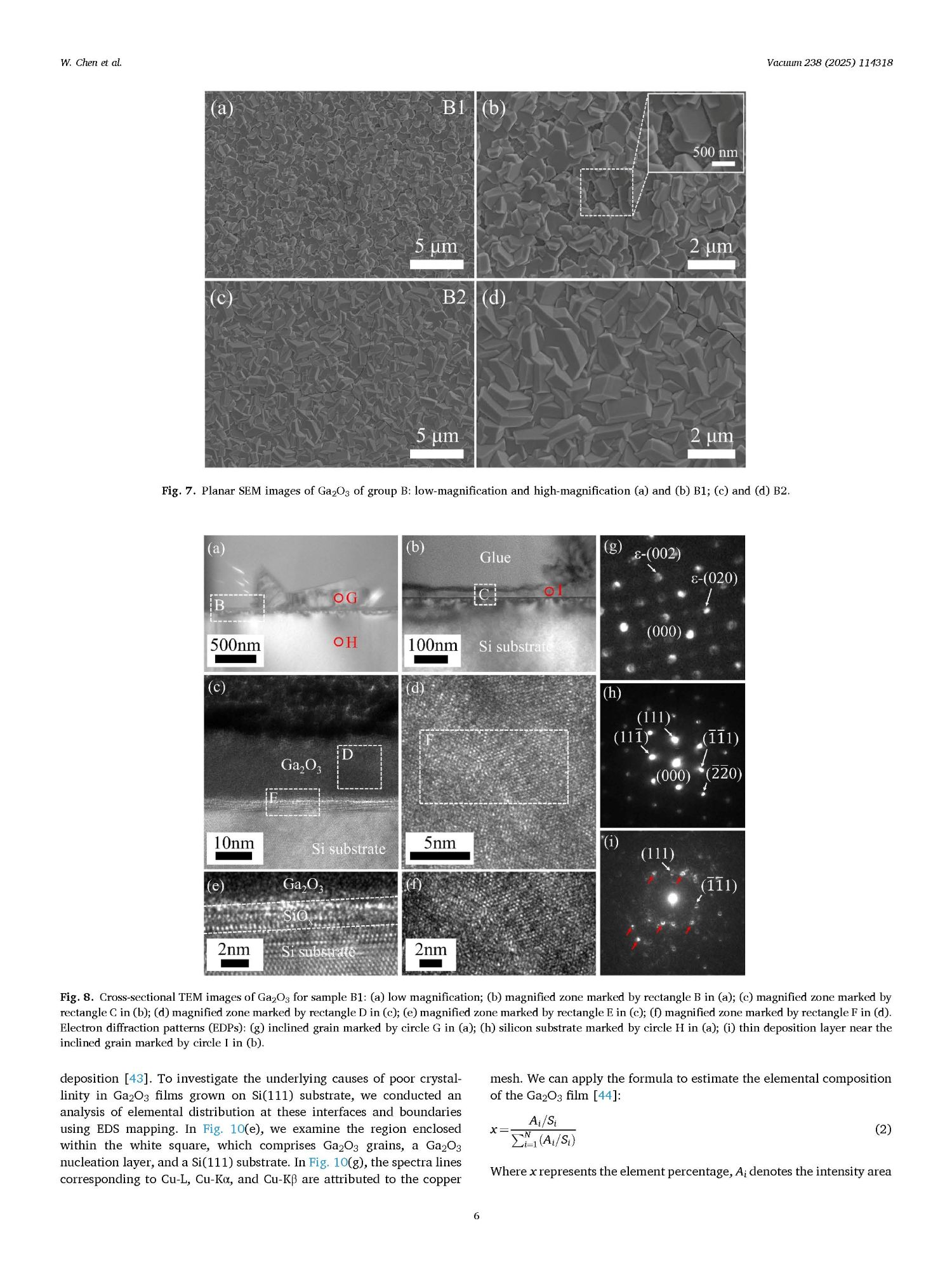
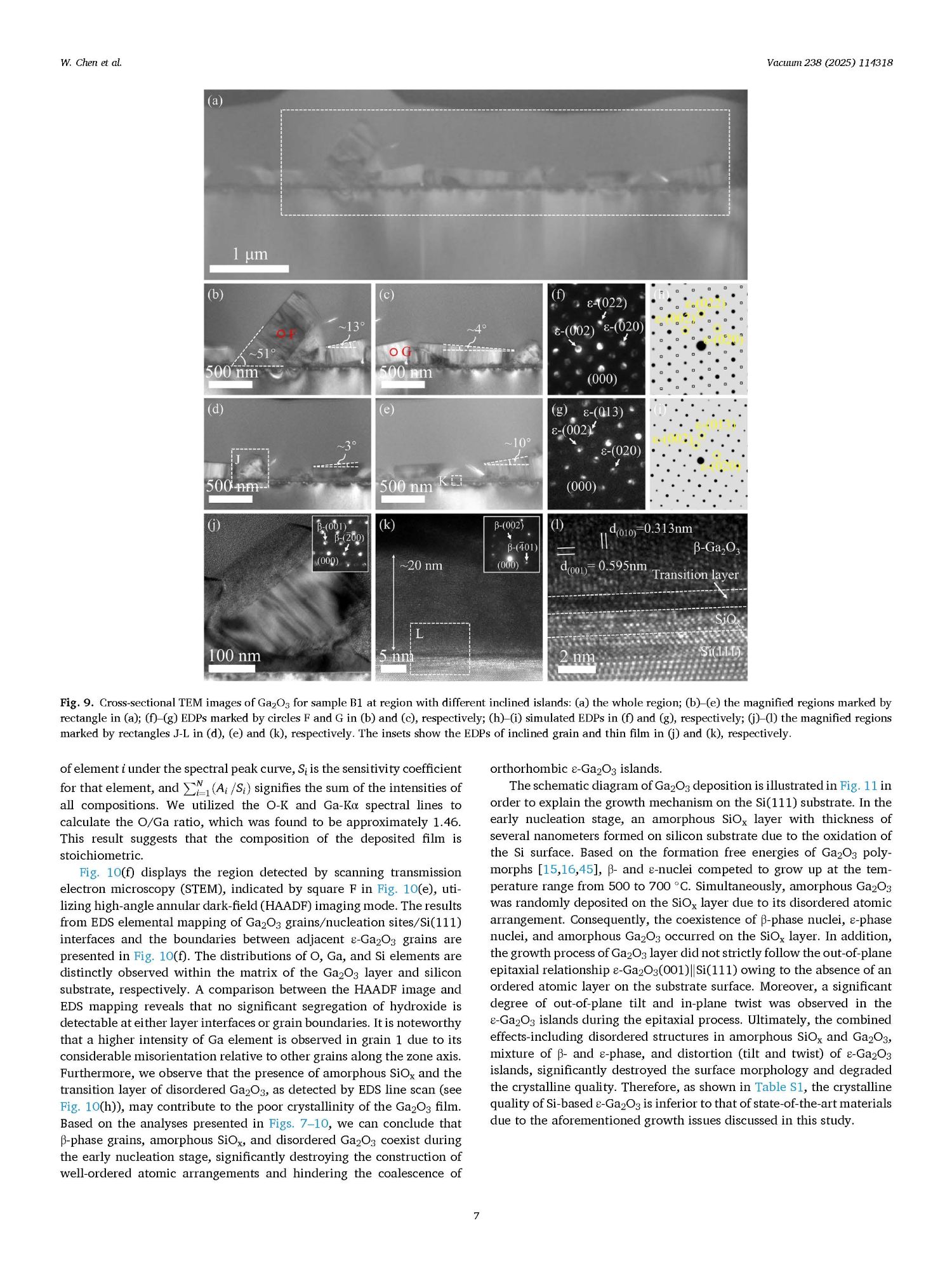
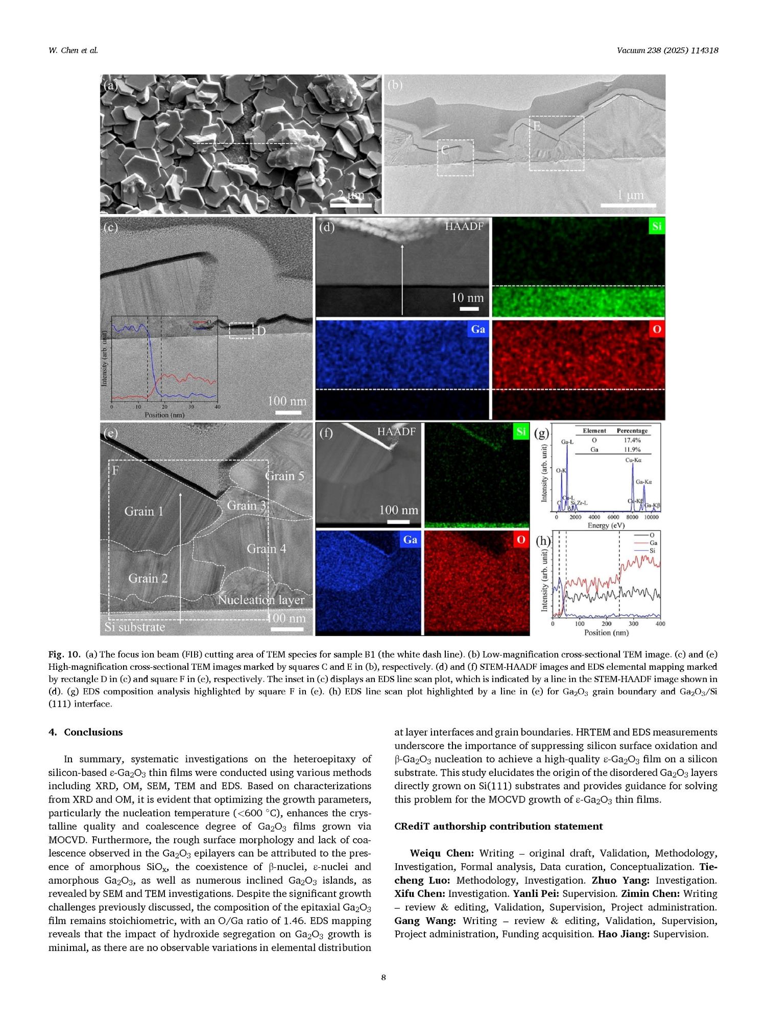
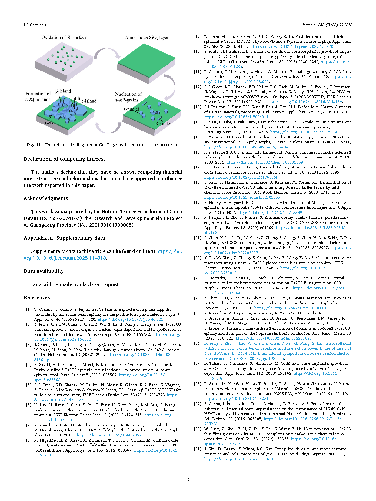
In summary, systematic investigations on the heteroepitaxy of silicon-based ε-Ga2O3 thin films were conducted using various methods including XRD, OM, SEM, TEM and EDS. Based on characterizations from XRD and OM, it is evident that optimizing the growth parameters, particularly the nucleation temperature (<600 °C), enhances the crystalline quality and coalescence degree of Ga2O3 films grown via MOCVD. Furthermore, the rough surface morphology and lack of coalescence observed in the Ga2O3 epilayers can be attributed to the presence of amorphous SiOx, the coexistence of β-nuclei, ε-nuclei and amorphous Ga2O3, as well as numerous inclined Ga2O3 islands, as revealed by SEM and TEM investigations. HRTEM and EDS measurements underscore the importance of suppressing silicon surface oxidation and β-Ga2O3 nucleation to achieve a high-quality ε-Ga2O3 film on a silicon substrate. This study elucidates the origin of the disordered Ga2O3 layers directly grown on Si(111) substrates and provides guidance for solving this problem for the MOCVD growth of ε-Ga2O3 thin films.
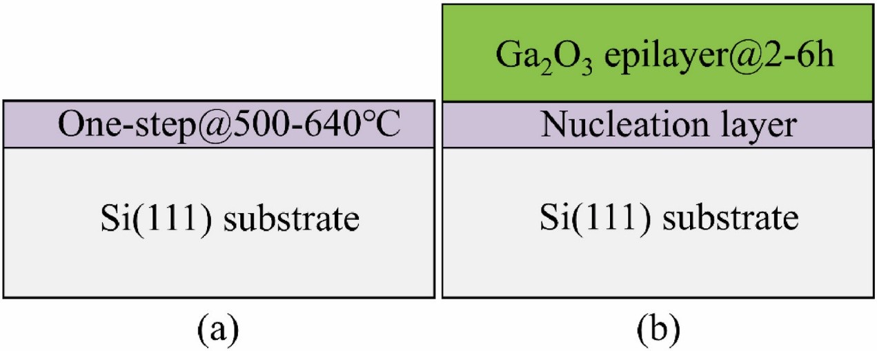
Fig. 1. Schematic diagrams of epitaxial structure grown on Si(111) substrates: (a) Sample A1-A4; (b) Sample B1-B2.
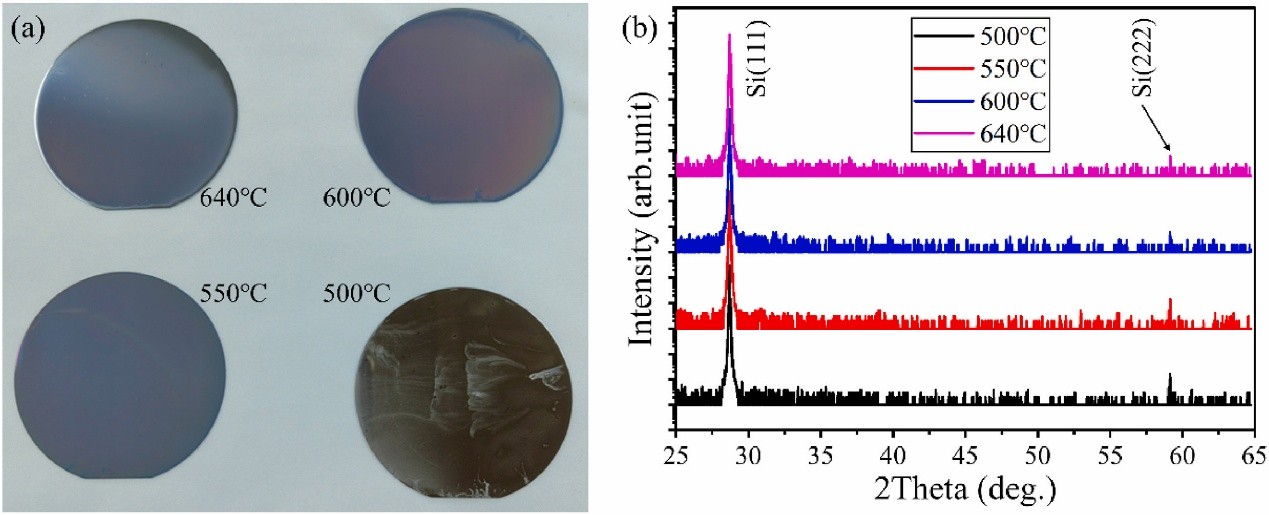
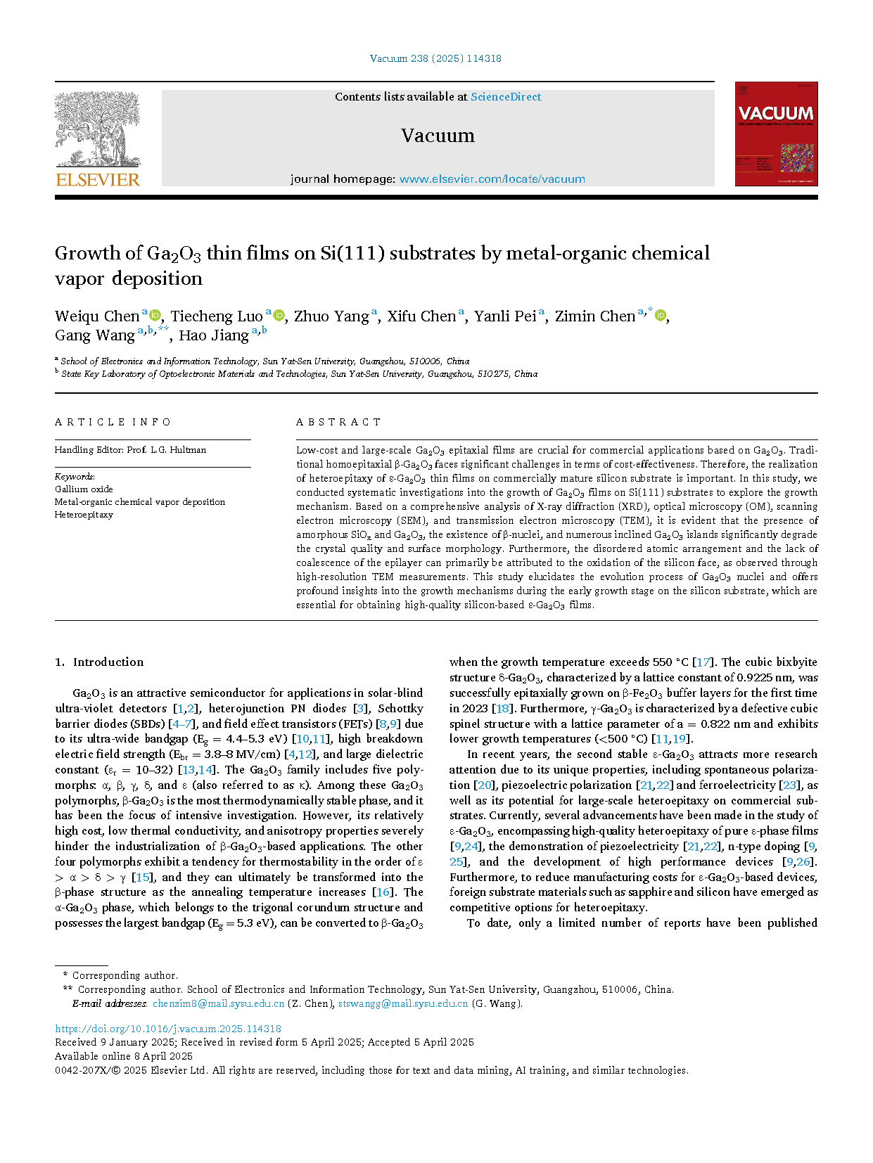
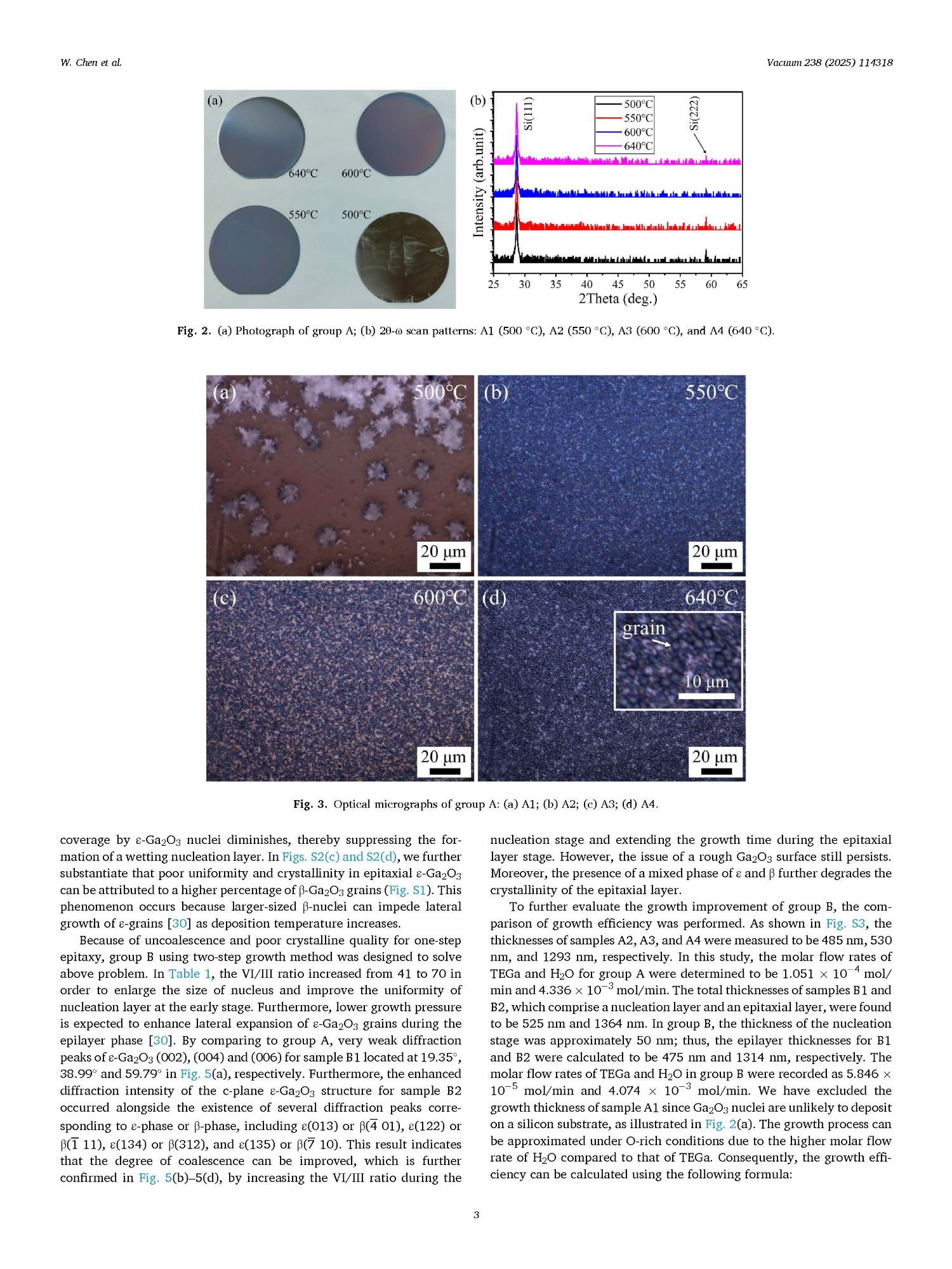
Fig. 2. (a) Photograph of group A; (b) 2θ-ω scan patterns: A1 (500 °C), A2 (550 °C), A3 (600 °C), and A4 (640 °C).
DOI:
doi.org/10.1016/j.vacuum.2025.114318