


News Trends
【World Express】Gallium Oxide, Controlled by the United States: Japan Goes Ahead, China Has A Breakthrough
日期:2023-03-14阅读:1743
Gallium Oxide is One of the Most Promising Materials in the Future.

Recently, the U.S. Department of Commerce's Bureau of Industry and Security established export controls on four technologies that are considered to be emerging and fundamental, which includes gallium oxide (Ga2O3), a substrate of ultra wide band gap semiconductor. Like other compound semiconductors such as silicon carbide (SiC) and gallium nitride (GaN), gallium oxide is a wide band gap semiconductor with potential applications in power switches and radio frequency electronic devices. Gallium oxide stands out in its wider gap of 4.8 electron volts (eV). In contrast, the band gap of GaN is 3.4eV, SiC is 3.26eV, and silicon is only 1.1eV.
Great Potential of Gallium Oxide
Among the five characteristics that are important to semiconductors, the high critical electric field strength is the greatest advantage of β-Ga2O3. This helps to produce high-voltage switches and may also be used in powerful RF equipment. A major weakness of β-Ga2O3 is its low thermal conductivity, which means that heat will be kept inside the equipment.
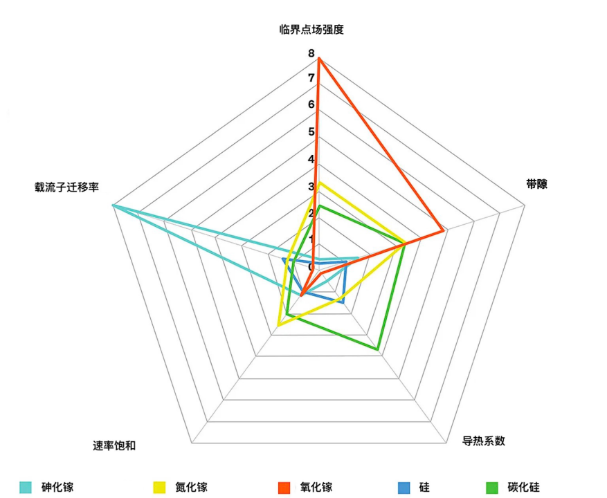
GREGGH.JESSEN等人在2017年第75届年度设备研究会议(DRC)上发表“TOWARD REALIZATION OF GA2O3 FOR POWER ELECTRONICS APPLICATIONS”。
Compared with other wide band gap semiconductors, gallium oxide has many characteristics that make it compatible with commercial production processes. For example, like silicon, gallium oxide can also be doped by an ion implantation process. Most importantly, gallium oxide wafers can be manufactured by commercial crystal growth technologies, such as the Czochralski method. This is different from GaN, which must be grown on silicon, SiC or sapphire substrates. There is a risk of damage caused by lattice mismatch.
Ga2O3-based semiconductor power devices, such as Schottky barrier diodes and transistors, are being studied in the industry. Deep ultraviolet photodetectors is included in other applications .
Gallium Oxide Research, Japan goes ahead
As a matter of fact, the pioneering research on gallium oxide was mainly conducted in Japan, followed by Germany and the United States. In 2012, Masataka Higashiwaki of the National Institute of Information and Communication Technology (NICT) of Japan took the lead in using the most stable β-Ga2O3 crystal to make Ga2O3 transistor, which is called metal semiconductor field-effect transistor.
At the same time, the National Institute of Materials Science of Japan and the Leibniz-Institute für Kristallzüchtung (IKZ) also led the study on β-Ga2O3. In 2015, NICT and Tamura co-founded the company Novel Crystal Technology (NCT), which successfully demonstrated 150mm β-Ga2O3 wafer. It is reported that NCT and FLOSFIA, a company separated from Kyoto University in 2011, are one of the two companies in the world that can mass produce Ga2O3 materials and components, establishing Japan's leading position in this emerging field.
"The first power device using Ga2O3 will be Schottky barrier diode (SBD). We are developing SBD with the goal of starting sales in 2022," said Takekazu Masui, senior executive and senior sales manager of NCT. NCT is also developing high-voltage vertical transistors based on this technology. NCT has overcome some of the challenges of gallium oxide. "With regard to thermal conductivity, NCT has confirmed that by making components thinner like other semiconductors, we can obtain thermal resistance that can be put into practical use. NCT is developing two p-type methods. One is to make gallium oxide p-type, and the other is to use nickel oxide, copper oxide and other oxide semiconductors as p-type materials.
The United States has also conducted researches in this field. On the basis of the success of NICT, the U.S. Air Force Research Laboratory (AFRL) has made some milestone achievements in gallium oxide research, including demonstrating the possibility of manufacturing normally-off FETs. Although gallium oxide lacks p-type carriers, which is a major obstacle in the industry, AFRL also buys substrates from Tamura and epitaxial wafers from NCT and IKZ.
Research Progress of Gallium Oxide in China
In China, the research on gallium oxide has been carried out for ten years, and there has been a breakthrough in recent years. Hao Yue, an academician of the CAS Member, clearly pointed out in an interview that gallium oxide material is one of the most promising materials in the future. In the next 10 years or so, gallium oxide devices are likely to become competitive power electronic devices and directly compete with silicon carbide devices.
In May 2022, Zhejiang University Hangzhou Science and Technology Innovation Center announced that the Advanced Semiconductor Research Institute of the Center had invented a new melt method technology to develop Ga2O3 bulk single crystals and wafers. At present, Ga2O3 wafers with a diameter of 2 inches (50.8 mm) have been successfully produced. Domestic institutions and universities that are studying gallium oxide also include Xi'an University of Electronic Science and Technology, Shanghai Institute of Optics and Mechanics, Shanghai Institute of Microsystems, Fudan University, Nanjing University, Shandong University, etc. The 46th Research Institute of China Electronics Technology Group Corporation has successfully produced the first 100 mm single crystal Ga2O3 wafer in China.
At the same time, there are also start-ups focusing on gallium oxide. The "Hard Science and Technology" industrialization platform jointly built by Shanghai Institute of Optics and Precision Machinery, Chinese Academy of Sciences, and the government of Fuyang District, ----Hangzhou Fujia Gallium Industry, a scientific and technological enterprise incubated by Hangzhou Institute of Optics and Mechanics.
Some analysts predict that the market size of Ga2O3 power semiconductor will reach 1.5 billion US dollars by 2030. In September 2017, gallium oxide was listed in the key research and development plan by the High-Tech Department of the Ministry of Science and Technology; In March 2018, Beijing Municipal Science and Technology Commission took the lead in conducting research on cutting-edge new materials, and listed gallium oxide as a key project. In addition, Anhui and other provinces/cities also proposed to research and develop wide band gap semiconductor materials, processes, devices and chips, such as gallium oxide, in the major special projects of integrated circuits announced in "the Fourteenth Five-Year Plan of Science and Technology Innovation.
