Member News
【Member News】 New Breakthrough | GAREN SEMI Successfully Prepared 100mm (010) planar Gallium Oxide Single Crystal Substrate by VB Method
日期:2025-06-12阅读:1076
In May 2025, Hangzhou GAREN SEMI Co., LTD. (hereinafter referred to as GAREN SEMI) made a breakthrough in the growth of large-sized Gallium Oxide crystals and substrate processing technology. Based on its independently developed Gallium Oxide dedicated crystal growth equipment, it fabricated a 100-millimeter (010) planar Gallium Oxide single crystal substrate using the Vertical Bridgeman (VB) method. This achievement is the first of its kind to be reported internationally.
Previously, GAREN SEMI successfully grew a 100-millimeter Gallium Oxide single crystal using the Vertical Bridgeman (VB) method. After process iteration and optimization, the preparation of a 100-millimeter (010) planar Gallium Oxide single crystal substrate was successfully achieved, and characterization tests were carried out simultaneously. The test results show that there is no twin in the substrate, the FWHM of the single crystal substrate XRD rocking curves is less than 50 arcsec, the RMS of the substrate is less than 0.1 nm, and the quality reaches the international advanced level.
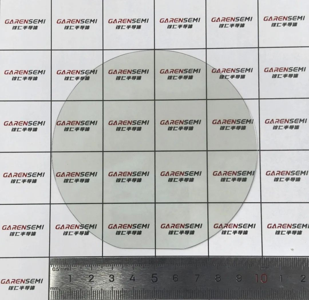
[Figure 1] GAREN SEMI VB method
100 mm (010) planar Gallium Oxide single crystal substrate
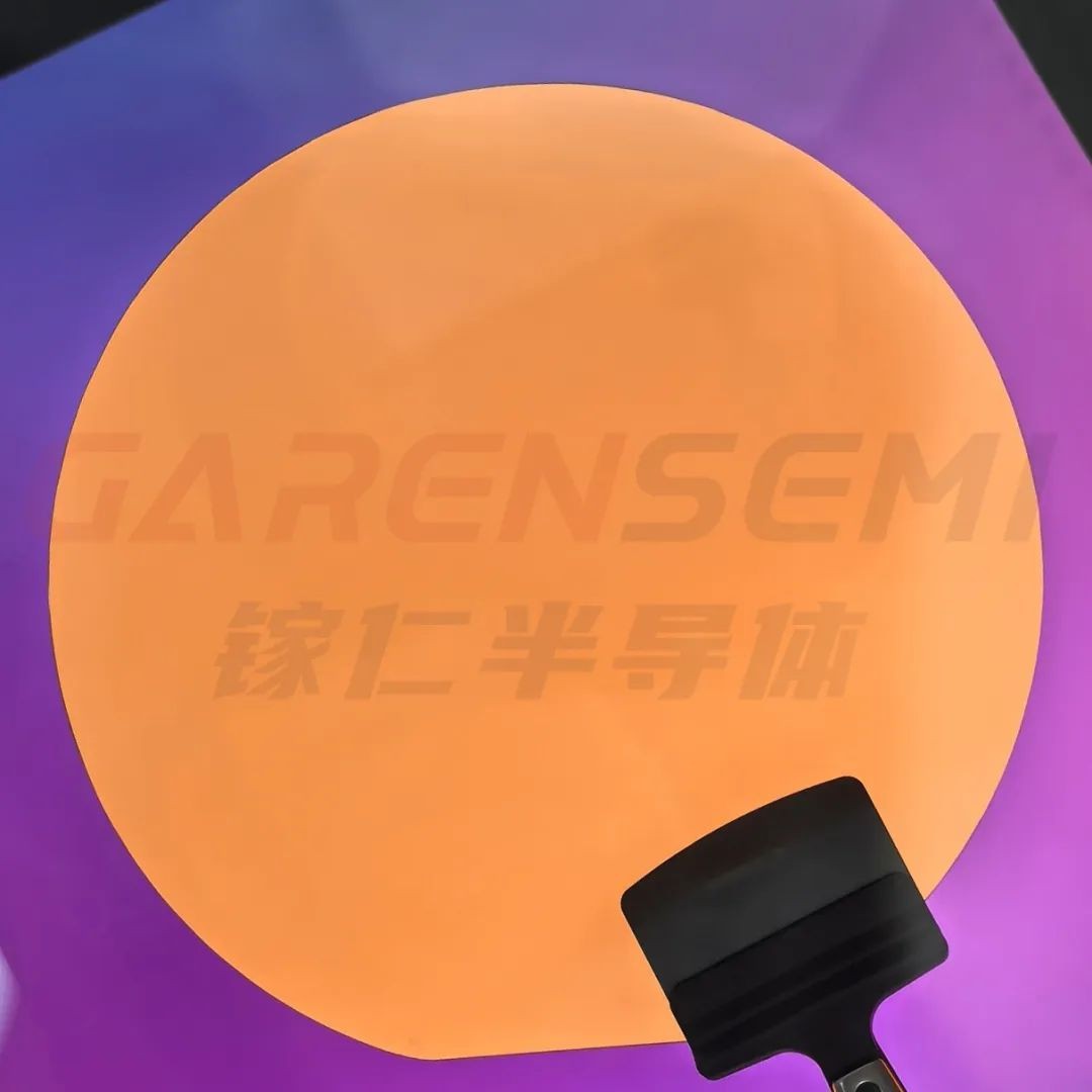
[Figure 2] GAREN SEMI VB method
Polarizing micrograph of 100 mm (010) planar Gallium Oxide single crystal substrate
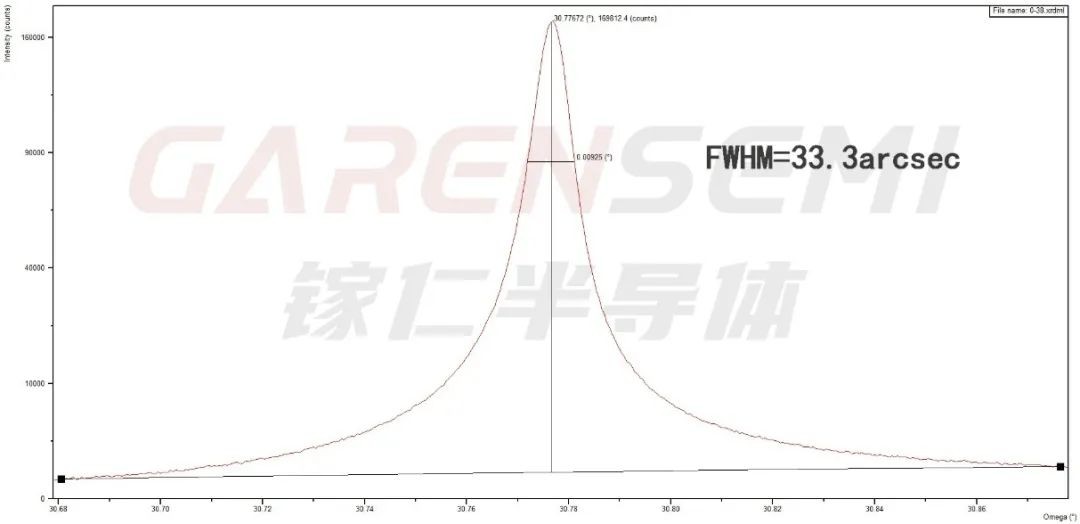
[Figure 3] GAREN SEMI VB method
XRD data of 100 mm (010) planar Gallium Oxide single crystal substrate
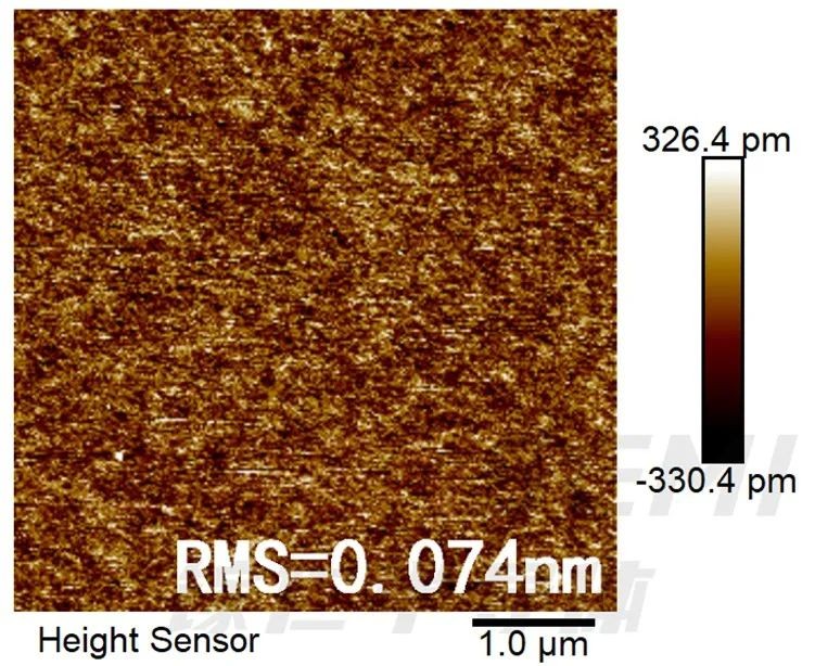
[Figure 4] GAREN SEMI VB method
AFM data of 100 mm (010) planar Gallium Oxide single crystal substrate
01 Why Has Gallium Oxide Become a New Direction for Ultra-Wide Band Gap Semiconductors?
In recent years, with the rapid development of new energy, photovoltaic power generation, radar detection, 5G mobile communication and other fields, ultra-wide band gap semiconductor materials represented by Gallium Oxide have begun to attract extensive attention and emphasis from all walks of life. Gallium Oxide has unique advantages over other compound semiconductors. Let's take the widely used Gallium Nitride as an example for comparison.
1.Gallium Oxide has a higher working voltage and power: The bandgap of Gallium Oxide single crystal is approximately 4.8eV, and the breakdown electric field strength is about 8MV/cm, which is much greater than that of Gallium Nitride (3.4eV, 3.3MV/cm). The power devices made from it have a higher working voltage and power.
2.Gallium Oxide devices have lower energy loss: The Baliga’s Figure of Merit of Gallium Oxide is approximately 3444, which is about four times that of Gallium Nitride. This means that devices developed using Gallium Oxide will have smaller on-resistance and higher power conversion efficiency.
3.Gallium Oxide can simultaneously meet the requirements of high frequency and high power: Gallium Oxide has a large Johnson's Figure of Merit (2844), which is more advantageous than Gallium Nitride (1089). It can simultaneously meet the requirements of high frequency and high power and has broad prospects in the field of radio frequency.
4.Gallium Oxide has excellent ultraviolet photoelectric properties: The ultraviolet cut-off wavelength of Gallium Oxide single crystal is approximately 260nm, which is shorter than that of Gallium Nitride (about 365nm), and the transmittance in the ultraviolet band is less affected by carrier concentration, thus having obvious advantages in the preparation of deep ultraviolet photoelectric devices.
5.Gallium Oxide has stronger thermal and chemical stability: Compared with Gallium Nitride, Gallium Oxide is more resistant to high temperatures and has better stability in extreme environments. It has obvious advantages in the manufacture of high-voltage power devices, RF devices, deep ultraviolet optoelectronic components, etc.
02 What are the Advantages of Selecting the (010) Surface for Gallium Oxide Growth?
Among the common mainstream crystal planes of Gallium Oxide single crystal substrates, (010) substrates exhibit outstanding performance in terms of physical properties and epitaxy:
1.The (010) substrate has the highest thermal conductivity, which is beneficial for improving the performance of power devices;
2.The (010) substrate has a fast epitaxial growth rate and good epitaxial matching, making it the preferred epitaxial crystal plane.
At present, GAREN SEMI has launched a wafer-level (010) Gallium Oxide single crystal substrate product. This product is targeted at the scientific research market, meeting the demand for (010) substrates in the scientific research field and promoting the collaborative cooperation among industry, academia and research.
03 Why Use VB Method for the Growth of Gallium Oxide Single Crystal?
The VB method has significant advantages in the growth of Gallium Oxide single crystal and is becoming the new favorite in the industry. Both domestic and foreign Gallium Oxide substrate manufacturers have begun to lay out their plans..
Advantage 1: The VB method is suitable for growing Gallium Oxide single crystal with an axial direction parallel to the [010] crystal direction, which is conducive to processing large-sized (010) face single crystal substrates.
Advantage 2: The VB method does not use the precious metal iridium crucible, and there is no need to consider the oxidation loss of the crucible. Compared with the common growth methods that use iridium crucibles, the cost is significantly reduced.
Advantage 3: The VB method can grow single crystal in an air atmosphere, which can effectively inhibit the high-temperature decomposition of Gallium Oxide, reduce defects such as inclusions in the crystal due to crucible corrosion, and improve the quality of the crystal.
Advantage 4: The VB method has a small temperature gradient, resulting in fewer dislocations induced by thermal stress in the crystal and higher crystal quality.
Advantage 5: VB crystals grow in the crucible, and the crystal diameter is the same as the crucible diameter. Therefore, there is no need to control the crystal diameter, the technical difficulty is low, the stability is high, and it is easy to achieve automatic control.
04 What Equipment is Used for Growing Gallium Oxide by the VB Method?
In September 2024, GAREN SEMI launched its first self-developed crystal growth equipment dedicated to Gallium Oxide. This equipment not only meets the requirements of high-temperature and high-oxygen environments for Gallium Oxide growth but also enables fully automated crystal growth, reducing manual intervention and significantly enhancing production efficiency and crystal quality.
This equipment can obtain large-sized single crystal with various crystal planes through process control, and supports upgrades to even larger single crystal, meeting the various demands of universities, research institutes, and enterprise customers for the growth of Gallium Oxide crystals in terms of research and production. This type of Gallium Oxide VB method crystal growth equipment and its process package have been fully opened.
Company Profile
Hangzhou GAREN SEMI Co., Ltd. was established in September 2022. It is a technology-based enterprise specializing in the research and development, production and sales of wide bandgap semiconductor materials and equipment such as Gallium Oxide.
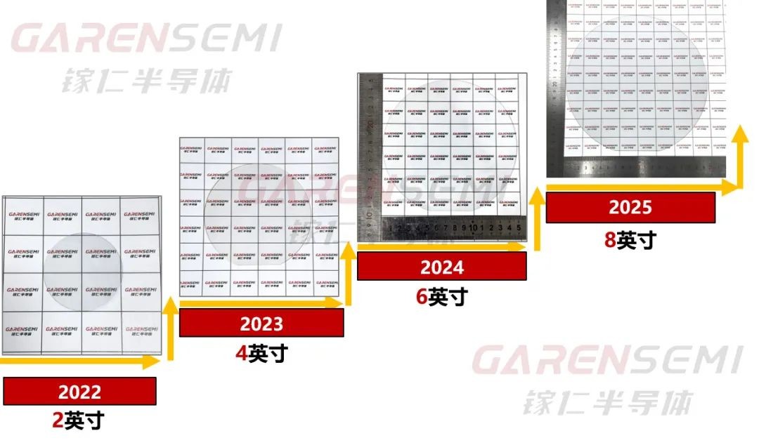
GAREN SEMI leads industry innovation by adopting its independently developed new casting method for single crystal growth technology. It was the world's first to launch an 8-inch Gallium Oxide single crystal substrate, setting an industry record of upgrading one size each year from 2 inches to 8 inches. And have developed the first domestic VB crystal growth equipment dedicated to Gallium Oxide that includes a process package and are now fully available for sale. GAREN SEMI is committed to addressing major national demands. It has mastered core technologies covering the entire chain of Gallium Oxide growth, processing, and epitaxy, and has obtained 14 domestic and international invention patents. It is deeply engaged in continuous innovation in the upstream industrial chain of Gallium Oxide.
The company's products include Gallium Oxide substrates of different sizes, crystal orientations and resistivity, as well as customizable Gallium Oxide seed crystals, etc. The products are mainly used in power electronic devices for the state grid, new energy vehicles, rail transit, 5G communication and other fields. After years of research and development, the company has mastered the core technologies of the entire chain, including equipment development, thermal field design, crystal growth, and crystal processing, and is capable of providing Gallium Oxide substrates with completely independent intellectual property rights. GAREN SEMI is committed to addressing major national demands. It will focus on continuous innovation in the upstream industrial chain of Gallium Oxide and strive to provide product support for the development of China's power electronics and other industries.
For more information about GAREN SEMI and its products
Please visit our official website: http://garen.cc/
Or contact us by:
Mr. Jiang :15918719807
Email :jiangjiwei@garen.cc
Mr. Xia :19011278792
Email :xianing@garen.cc