


Discover
【Knowledge Discover】Gallium Oxynitride Materials: Versatile in "Gallium System" Material Devices
日期:2025-06-16阅读:2011
1、Basic Properties of Gallium Oxide Materials: Adjustable Wide Band Gap and Multi-Functional Characteristics
Gallium Oxynitride (GaOxNy) is a compound that lies between the crystalline and amorphous states. Its physical and chemical properties can be continuously adjusted between Gallium Nitride (GaN) and Gallium Oxide (Ga2O3) by regulating the preparation conditions. It combines the characteristics of wide band gap semiconductors with flexible functional design, and thus shows unique advantages in power electronics, ultraviolet optoelectronic devices, and photoelectrocatalysis fields [1-2].
Crystal structure diversity: The crystal structure of GaON includes amorphous, β phase (Ga2ON3), γ phase (Ga3O3N), and hexagonal GaOxN1-x, etc. Its structure and properties are highly dependent on the synthesis process [1].
Band engineering potential: The Bandgap (Eg) is between that of GaN (3.4 eV) and Ga2O3(4.5–4.9 eV)and can be precisely controlled by adjusting the oxygen nitrogen ratio.
Interface optimization characteristics: GaON has high lattice matching with GaN and can serve as an intermediate layer in heterojunctions, suppressing Metal-Induced Gap States (MIGS) and interface dangling states, and improving device interface quality [7].
Selective oxidation process: Based on the thermodynamic property that GaN is more easily oxidized than InAlN, the GaON functional layer can be precisely prepared through oxidation reactions without damaging the InAlN barrier layer [8].
2、 Preparation Method of Gallium Oxide Materials
Plasma injection oxidation: Oxygen plasma is injected into the GaN lattice, and after annealing, oxygen atoms replace nitrogen atoms to form hexagonal GaOxNy nanolayers [2].
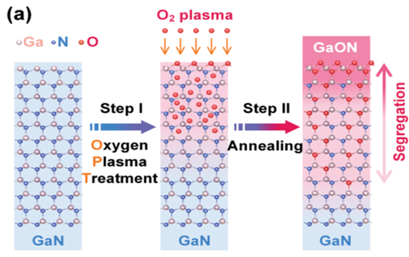
Preparation method of hexagonal GaOxNy formed by Oxygen Plasma Treatment (OPT)+annealing
RF magnetron sputtering oxidation: Using Ga2O3 as the target material, component control is achieved by adjusting the N2/O2 plasma ratio, combined with vacuum annealing to optimize the crystal structure, as shown in the phase diagram below [1]:
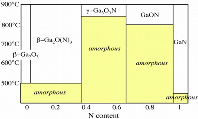
Preparation method of hexagonal GaOxNy formed by RF magnetron sputtering and vacuum annealing
Annealing: High-temperature annealing of the GaN surface in an oxygen-containing atmosphere directly generates GaON layers, a simple process that is compatible with existing device processes [9].
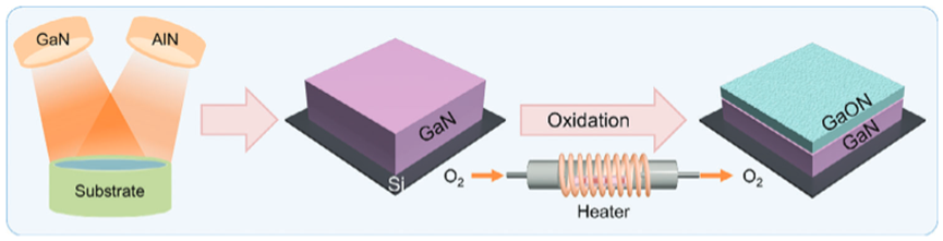
Method for preparing GaON by oxygen atmosphere annealing
3、Core Applications: From Power/Radio Frequency Electronics to Ultraviolet Optoelectronics
The Field of Power Electronic Devices:
Introducing GaON nanolayers beneath the cathode metal layer of p-GaN Schottky diodes (SBD) can enhance the reverse breakdown characteristics. By taking advantage of the valence band step difference (~ 0.5 eV) between GaON and GaN, the reverse injection of holes is prevented, reducing the leakage current by two orders of magnitude while maintaining a low on-resistance (Ron) [2].
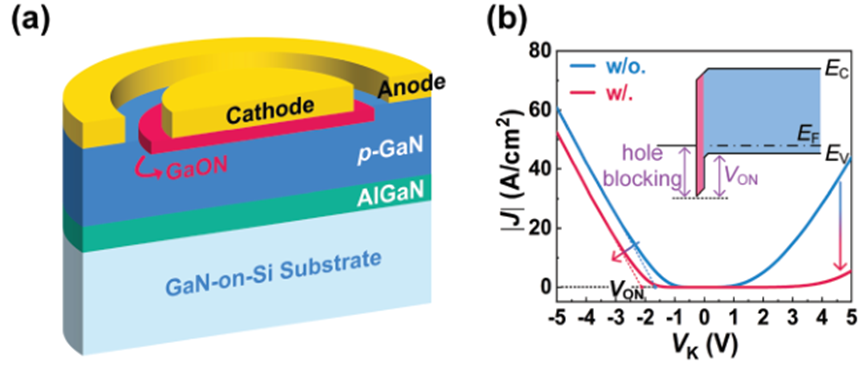
The role of introducing GaON layers beneath the cathode of p-GaN SBD
The Field of Radio Frequency Electronic Devices:
In GaN high electron mobility transistors (HEMTs), the interface state (such as metal-induced gap state, MIGS) between the gate metal and the two-dimensional electron gas (2DEG) in the channel is a key bottleneck restricting high frequency performance. Traditional solutions often optimize interface quality through complex epitaxial structures or expensive substrates (such as Silicon Carbide), but they have problems such as high process costs and limited scalability. The innovative process based on GaON materials by the team led by Zhang Yun from the Institute of Semiconductors, Chinese Academy of Sciences, has provided a brand-new approach to this challenge:
1. The unique advantage of the selective oxidation process:
By using Oxygen Plasma Treatment (OPT), a 2 NNM thick GaN cap layer is precisely oxidized in the sub-gate region of the GaN/InAlN heterojunction to generate a GaON insertion layer. This process ingeniously takes advantage of the thermodynamic property that GaN is more easily oxidized than InAlN, enabling active regulation of the interface state without damaging the InAlN barrier layer [8]. This technological breakthrough avoids the damage to polarized charges caused by traditional etching or epitaxy processes, ensuring the high density and high migration characteristics of 2DEG.
2. Significant improvement in high-frequency performance:
With the introduction of the GaON layer, the gate leakage current is reduced by an order of magnitude, and the effective electron drift rate is increased to 2.2×107 cm/s (about 1.5×107 cm/s in conventional devices). The cut-off frequency (fT) and maximum oscillation frequency (fmax) of the device reached 240 GHz and 530 GHz respectively, which is comparable to the performance of Silicon Carbide substrate devices. For the first time, ultra-high frequency performance with a Ka-band noise figure of less than 0.98 dB and a W-band linear gain of 8 dB was achieved on a low-cost sapphire substrate [8]. This achievement breaks through the limitations of substrate materials for high-frequency devices, making it possible for large-scale commercialization.
3. Process compatibility and miniaturization potential:
Compared with the AlN/GaN superlattice interface optimization scheme that requires complex epitaxial stacking, the GaON insertion layer process only requires local oxidation modification and is highly compatible with the existing GaN HEMT production lines. In addition, the passivation effect of the GaON layer on the interface state significantly reduces the short-channel effect, enabling the device to achieve excellent frequency characteristics when miniaturized to sub-100 nm gate lengths, providing an expandable technical path for 5G/6G communications and terahertz technology.
Significance Summary: Redefining the Performance Boundaries of GaN HEMT
The introduction of GaON materials not only resolves the contradiction of "performance - cost - process" being difficult to achieve in traditional interface optimization techniques, but also promotes the leapfrog development of GaN HEMT technology through the following innovations:
1. Low-cost substrate high performance: Achieving RF indicators comparable to those of Silicon Carbide devices on sapphire substrates significantly lowers the threshold for commercialization.
2 Active control of interface states: Engineering nanoscale interfaces through selective oxidation to avoid damage to polarized charges by epitaxial processes.
3. High frequency - low noise - high power balance improvement: Breaking the trade-off between frequency and noise performance in traditional technology to lay the foundation for multifunctional integrated devices.
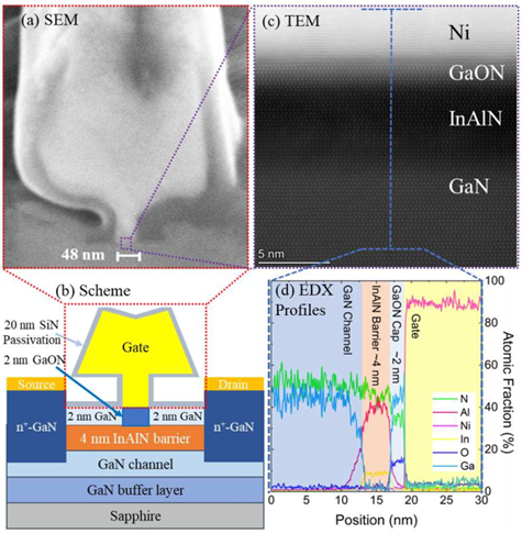
Introducing a GaON layer beneath the gate of a high-frequency GaN HEMT
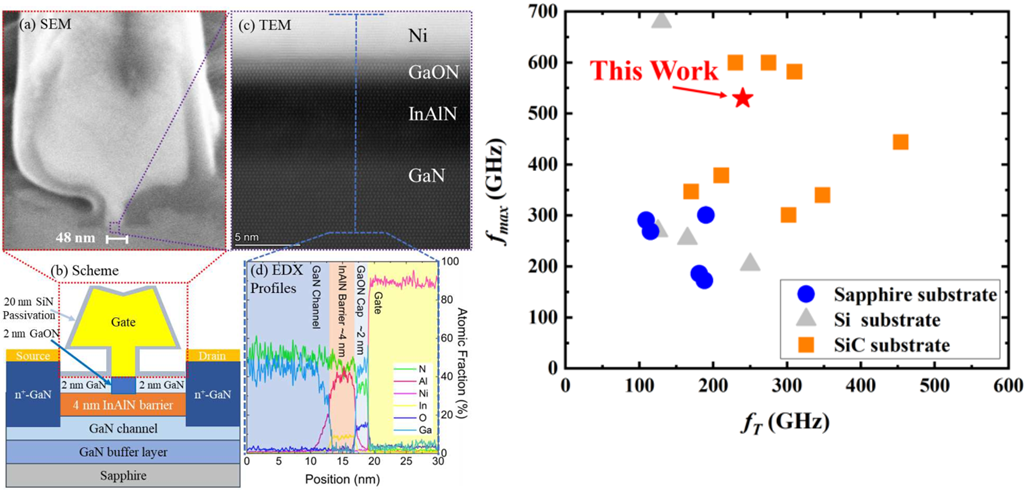
Comparison of bench marks for devices
The Field of Optoelectronic Devices:
1. Photoelectrocatalysis: Depositing a GaON layer on the surface of n-GaN can passivate surface defect and provide more catalytic active sites, significantly improving the efficiency of photoelectrochemical water splitting [10].
2. Ultraviolet detection: By introducing the GaON layer at the electrode interface of the p-GaN detector, the valence band step difference is utilized to block hole recombination, reducing the dark current to the order of 10−12 A and increasing the device sensitivity by three times [2].
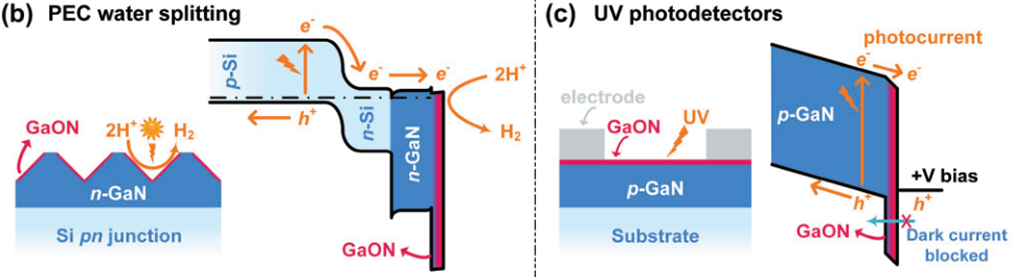
Left: The role of introducing the GaON layer in photocatalytic water splitting materials; Right: The role of introducing a GaON layer in a UV photodetector.
The Field of Interface Contact Technology:
In Gan-based devices, metal-semiconductor ohmic contact interface states (such as metal-induced interface states and dangling bond states) can lead to severe Fermi level pinning effects, causing contact resistivity (ρc) to remain at the 10−7Ω·cm2 order for a long time, becoming a major obstacle to device miniaturization and high frequency [7].
Innovative Solution for GaON Insertion Layer
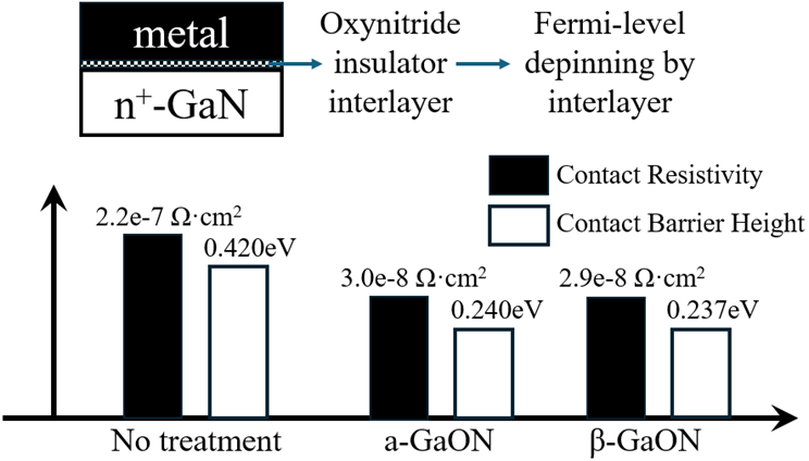
The team led by Zhang Yun from the Institute of Semiconductors, Chinese Academy of Sciences, has achieved the following breakthroughs by introducing a 2-3 nm thick GaON layer at the Ti/ N-gan interface through surface annealing process:
1. Interface state passivation: The GaON layer effectively passivates interface defect, alleviates Fermi level pinning, and reduces the contact barrier height from 0.42 eV to 0.24 eV.
2. Enhanced carrier tunneling: GaON aligns with the n-GaN conduction band (ΔEC≈ 0), which is beneficial for reducing tunneling resistance.
3. Process compatibility: Only an oxygen doping step needs to be introduced into the standard annealing process, without the need for complex epitaxy or patterned processes, seamlessly integrating with existing processes [7].
Core Significance: Redefining the Design Paradigm of Ohmic Contacts
1. Key support for miniaturization: Ultra-low ρc enables GaN devices to maintain low parasitic resistance at the nanoscale, breaking the miniaturization limit of high-frequency devices.
2. Universal innovation: This technology can be extended to the ohmic contact optimization of other wide band gap semiconductors (such as SiC, Ga2O3), providing a universal solution for contact resistance optimization in other material device fields.
The role of introducing GaON layer at Ti/n-GaN interface
4、Future Outlook: Material Innovation Drives Device Performance Upgrade
In-depth research on the application of Gallium Oxynitride materials not only resolves the bottlenecks of traditional GaN devices in interface states and high-frequency performance, but also provides brand-new solutions to key issues in fields such as ultraviolet optoelectronics, power electronics, and terahertz communication. With the maturation of the preparation process and the decline in costs, such materials are expected to support to the development of the next generation of semiconductor technologies.
References
[1] AKAZAWA H. Crystallization of gallium oxynitride thin films [J]. Journal of Solid State Chemistry, 2020, 282: 121066.
[2] CHEN J, ZHAO J, FENG S, et al. Formation and Applications in Electronic Devices of Lattice-Aligned Gallium Oxynitride Nanolayer on Gallium Nitride [J]. Advanced Materials, 2023, 35(12): 2208960.
[3] KING P D C, VEAL T D, KENDRICK C E, et al. InN/GaN valence band offset: High-resolution x-ray photoemission spectroscopy measurements [J]. Phys Rev B, 2008, 78(3): 033308.
[4] YUAN L, LI S, SONG G, et al. Solution-processed amorphous gallium oxide gate dielectric for low-voltage operation oxide thin film transistors [J]. Journal of Materials Science: Materials in Electronics, 2021, 32(7): 8347-53.
[5] SPENCER J A, MOCK A L, JACOBS A G, et al. A review of band structure and material properties of transparent conducting and semiconducting oxides: Ga2O3, Al2O3, In2O3, ZnO, SnO2, CdO, NiO, CuO, and Sc2O3 [J]. Appl Phys Rev, 2022, 9(1): 011315.
[6] ZVORISTE C. High-Pressure Synthesis, Crystal Structure and Physical Properties of Gallium Oxonitride [D]. Darmstadt; Technical University of Darmstadt, 2011.
[7] XIE S, HE J, WU X, et al. Achieving Ultralow Specific Contact Resistivity in Ti/n+-GaN Ohmic Contacts by Mitigating the FLP Effect with a Gallium Oxide Interlayer [J]. ACS Applied Electronic Materials, 2025, 7(7): 2709-19.
[8] HE J, CHENG Z, XIE S, et al. High-performance GaN HEMTs with GaON under-gate cap layer via barrier-friendly selective plasma oxidation [J]. Applied Physics Letters, 2025, 126(14): 143507.
[9] DAS D, SANCHEZ F, NALAM P G, et al. Effect of Thermal Oxidation on the Structure, Surface Texturing, and Microstructure Evolution in Nanocrystalline Ga─O─N Films [J]. Advanced Materials Interfaces, 2025, 12(5): 2400500.
[10] ZENG G, PHAM T A, VANKA S, et al. Development of a photoelectrochemically self-improving Si/GaN photocathode for efficient and durable H2 production [J]. Nature Materials, 2021, 20(8): 1130-5.
