Paper Sharing
【International Papers】Thermal transport in ion-beam-exfoliated β-Ga₂O₃ nanomembranes
日期:2025-06-18阅读:541
Researchers from the Nazarbayev University have published a dissertation titled "Thermal transport in ion-beam-exfoliated β-Ga2O3 nanomembranes" in APL Materials.
Abstract
β-Ga2O3 is a promising material for power electronics due to its wide bandgap and high breakdown field, but its low thermal conductivity poses challenges for heat dissipation. To address this, we employed ion beam exfoliation to fabricate β-Ga2O3 nanomembranes integrated with highly thermally conductive Si substrates. To do this, chromium ion implantation was used to induce stress and strain, forming rolled-up microtubes on (100)-oriented β-Ga2O3 single crystals. After successfully transferring these tubes onto Si substrates and performing thermal annealing, these microtubes were unrolled into nanomembranes. X-ray diffraction and Raman measurements revealed the high quality of the samples. Time-domain thermoreflectance was used to study thermal transport in these structures, confirming uniform thermal conductivity across three fabricated samples. A Debye-based thermal transport model was implemented to validate experimental results and define the main phonon scattering mechanisms. Non-equilibrium molecular dynamics simulations revealed that a thin amorphous SiO2 interlayer significantly enhanced the thermal boundary conductance (TBC) across the β-Ga2O3/Si interface by bridging the vibrational mismatch between β-Ga2O3 and Si. However, further increasing the interlayer thickness led to phonon scattering and reduced TBC, emphasizing the importance of precise interface thickness control. This study highlights ion beam exfoliation as a scalable approach for integrating β-Ga2O3 with thermally conductive substrates, providing a pathway to improved thermal management in β-Ga2O3-based power electronics.
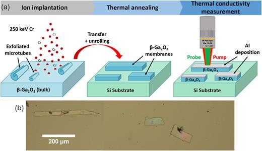
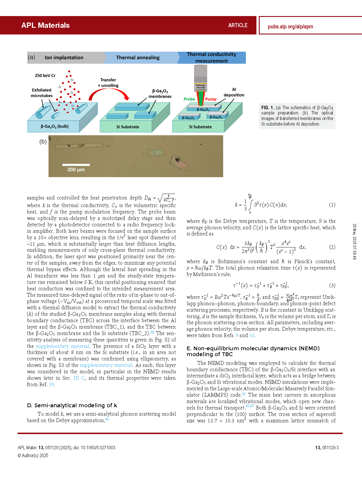
FIG. 1. (a) The schematics of β-Ga2O3 sample preparation. (b) The optical images of transferred membranes on the Si substrate before Al deposition.
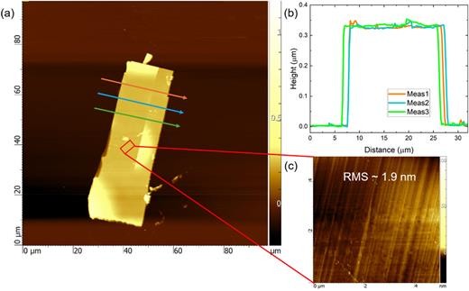
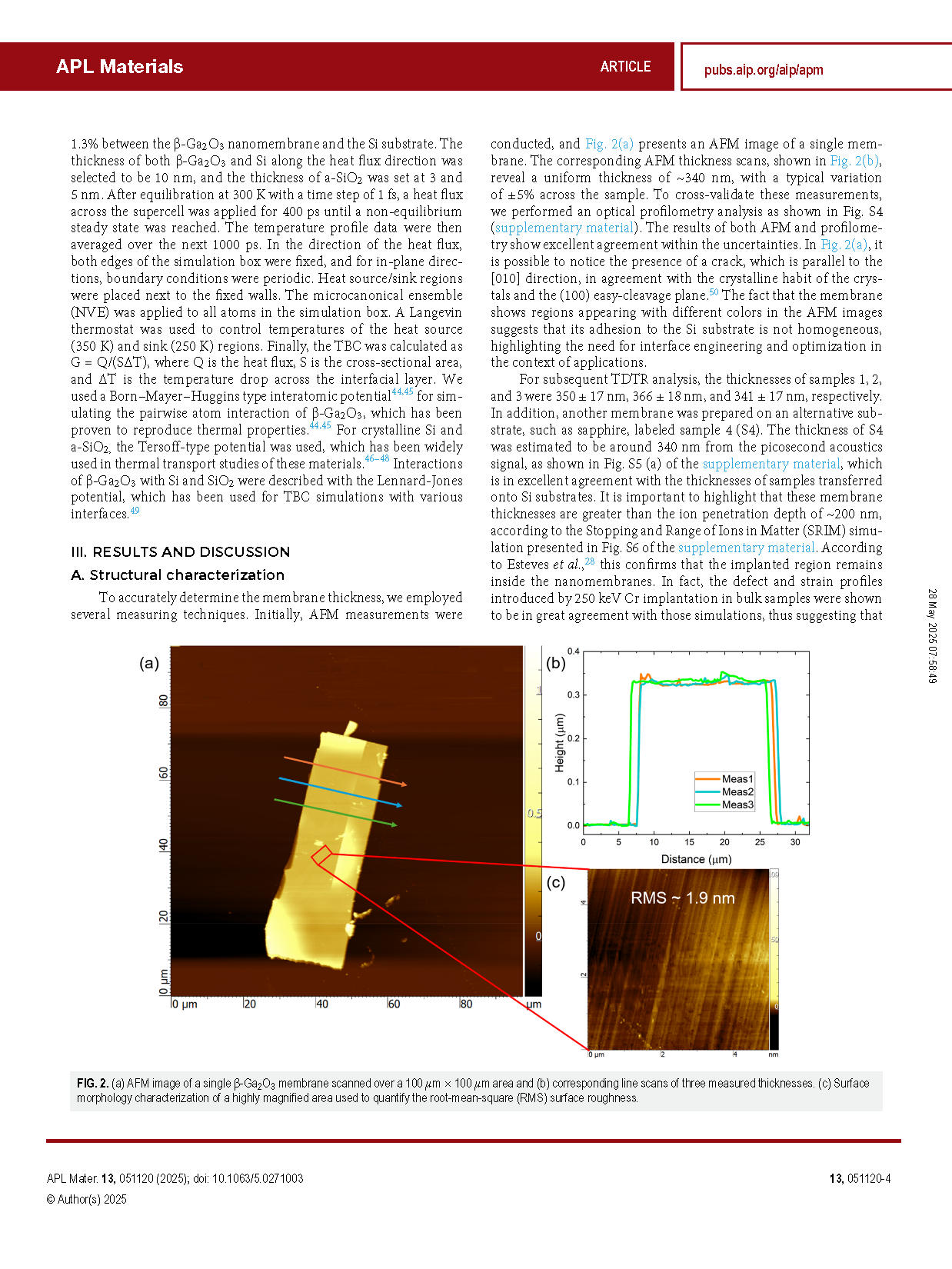
FIG. 2. (a) AFM image of a single β-Ga2O3 membrane scanned over a 100 μm × 100 μm area and (b) corresponding line scans of three measured thicknesses. (c) Surface morphology characterization of a highly magnified area used to quantify the root-mean-square (RMS) surface roughness.
DOI:
doi.org/10.1063/5.0271003